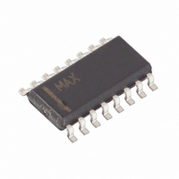
MAX3040CSE+ Maxim Integrated Products, MAX3040CSE+ Datasheet - Page 4

MAX3040CSE+
Manufacturer Part Number
MAX3040CSE+
Description
IC RS485/422 TRANS QUAD 16-SOIC
Manufacturer
Maxim Integrated Products
Type
Transmitterr
Datasheet
1.MAX3045BEUE.pdf
(15 pages)
Specifications of MAX3040CSE+
Number Of Drivers/receivers
4/0
Protocol
RS422, RS485
Voltage - Supply
4.75 V ~ 5.25 V
Mounting Type
Surface Mount
Package / Case
16-SOIC (3.9mm Width)
Data Rate
250 Kbps
Propagation Delay Time Ns
70 ns
Operating Supply Voltage
5 V
Supply Current
1 mA
Operating Temperature Range
0 C to + 70 C
Input Voltage
5 V
Maximum Power Dissipation
696 mW
Mounting Style
SMD/SMT
Output Current
+/- 25 mA to +/- 250 mA
Output Voltage
- 7.5 V to 12.5 V
Product
RS-422/RS-485 Combination
Ic Interface Type
RS422, RS485
No. Of Drivers
4
Supply Voltage Range
4.75V To 5.25V
Driver Case Style
SOIC
No. Of Pins
16
Filter Terminals
SMD
Rohs Compliant
Yes
Data Rate Max
250Kbps
Lead Free Status / RoHS Status
Lead free / RoHS Compliant
±10kV ESD-Protected, Quad 5V RS-485/RS-422
Transmitters
SWITCHING CHARACTERISTICS—MAX3041/MAX3044 (continued)
(V
SWITCHING CHARACTERISTICS—MAX3042B/MAX3045B
(V
4
Note 1: All currents into the device are positive; all currents out of the device are negative. All voltages are referenced to device
Note 2: ∆V
Note 3: This input current level is for the hot-swap enable (EN_, EN, EN) inputs and is present until the first transition only. After the
Note 4: Maximum current level applies to peak current just prior to foldback-current limiting. Minimum current level applies during
Driver Enable from Shutdown to
Output High
Driver Enable to Output Low
Driver Enable from Shutdown to
Output Low
Driver Disable Time from Low
Driver Disable Time from High
Maximum Data Rate
Driver Propagation Delay
Driver Differential Output
Rise-Time/Fall-Time
Skew Driver to Driver
Differential Driver Output Skew
| t
Driver Enable to Output High
Driver Enable from Shutdown to
Output High
Driver Enable to Output Low
Driver Enable from Shutdown to
Output Low
Driver Disable Time from Low
Driver Disable Time from High
CC
CC
PLH
_______________________________________________________________________________________
= +5V ±5%, T
= +5V ±5%, T
- t
ground unless otherwise noted.
first transition the input reverts to a standard high-impedance CMOS input with input current I
current may be as high as 1mA. During this period the input is disabled.
current limiting.
PHL
PARAMETER
PARAMETER
OD
|
and ∆V
A
A
= T
= T
OC
MIN
MIN
are the changes in V
to T
to T
MAX
MAX
t
ZH(SHDN)
t
, unless otherwise noted. Typical values are at V
, unless otherwise noted. Typical values are at V
SYMBOL
t
t
SYMBOL
ZH(SHDN)
ZL(SHDN)
ZL(SHDN)
t
t
DSKEW
SSKEW
t
f
SKEW
t
t
MAX
t
PLH
PHL
t
t
t
t
t
t
HZ
t
t
ZH
ZL
LZ
HZ
ZL
LZ
F
R
OD
Figures 2 and 3,
R
Figures 2 and 3,
R
Different chips
Same chip
Figures 2 and 3,
R
MAX3042B, Figures 4 and 5, S2 closed,
R
Figures 4 and 5, S2 closed,
R
MAX3042B, Figures 4 and 5, S1 closed,
R
Figures 4 and 5, S1 closed,
R
Figures 4 and 5, S1 closed,
R
Figures 4 and 5, S2 closed,
R
Figures 4 and 5, S2 closed,
R
MAX3041, Figures 4 and 5, S1 closed,
R
Figures 4 and 5, S1 closed,
R
Figures 4 and 5, S1 closed,
R
Figures 4 and 5, S2 closed,
R
and V
DIFF
DIFF
DIFF
L
L
L
L
L
L
L
L
L
L
L
= 500Ω, C
= 500Ω, C
= 500Ω, C
= 500Ω, C
= 500Ω, C
= 500Ω, C
= 500Ω, C
= 500Ω, C
= 500Ω, C
= 500Ω, C
= 500Ω, C
= 54Ω, C
= 54Ω, C
= 54Ω, C
OC
, respectively, when the transmitter input changes state.
L
L
L
L
L
L
L
L
L
L
L
= 100pF
= 100pF
= 100pF
= 100pF
= 15pF
= 15pF
CONDITIONS
DIFF
DIFF
DIFF
CONDITIONS
= 100pF
= 100pF
= 100pF
= 15pF
= 15pF
= 50pF
= 50pF
= 50pF
Figures 2 and 3,
R
C
DIFF
DIFF
= 54Ω,
= 50pF
CC
CC
= +5V and T
= +5V and T
MIN
MIN
20
A
A
IN
= +25°C.)
= +25°C.)
. For the first 20µs the input
TYP
TYP
23
23
±8
MAX
MAX
400
400
400
500
500
300
300
300
300
400
400
40
40
17
17
±8
±8
UNITS
UNITS
Mbps
ns
ns
ns
ns
ns
ns
ns
ns
ns
ns
ns
ns
ns
ns
ns


