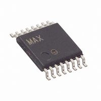
MAX3043EUE+ Maxim Integrated Products, MAX3043EUE+ Datasheet - Page 9

MAX3043EUE+
Manufacturer Part Number
MAX3043EUE+
Description
IC RS485/422 TRANS QUAD 16TSSOP
Manufacturer
Maxim Integrated Products
Type
Transmitterr
Datasheet
1.MAX3045BEUE.pdf
(15 pages)
Specifications of MAX3043EUE+
Number Of Drivers/receivers
4/0
Protocol
RS422, RS485
Voltage - Supply
4.75 V ~ 5.25 V
Mounting Type
Surface Mount
Package / Case
16-TSSOP
Lead Free Status / RoHS Status
Lead free / RoHS Compliant
The stresses are applied while the MAX3040–MAX3045
are powered up. Test results are reported as:
1) Normal performance within the specification limits.
2) Temporary degradation or loss of function or perfor-
3) Temporary degradation, loss of function or perfor-
4) Degradation or loss of function not recoverable due
The MAX3040–MAX3045 meets classification 2 listed
above. Additionally, the MAX3040–MAX3045 will not
latchup during the IEC burst stress events.
When circuit boards are plugged into a “hot” back-
plane, there can be disturbances to the differential sig-
nal levels that could be detected by receivers
connected to the transmission line. This erroneous data
could cause data errors to an RS-485/RS-422 system.
To avoid this, the MAX3040–MAX3045 have hot-swap
capable inputs.
When a circuit board is plugged into a “hot” backplane
there is an interval during which the processor is going
through its power-up sequence. During this time, the
processor’s output drivers are high impedance and will
be unable to drive the enable inputs of the
MAX3040–MAX3045 (EN, EN, EN_) to defined logic lev-
els. Leakage currents from these high impedance dri-
vers, of as much as 10µA, could cause the enable
inputs of the MAX3040–MAX3045 to drift high or low.
Additionally, parasitic capacitance of the circuit board
could cause capacitive coupling of the enable inputs to
either GND or V
enable inputs of the MAX3040–MAX3045 to drift to lev-
els that may enable the transmitter outputs (Y_ and Z_).
To avoid this problem, the hot-swap input provides a
method of holding the enable inputs of the
MAX3040–MAX3045 in the disabled state as V
ramps up. This hot-swap input is able to overcome the
leakage currents and parasitic capacitances that may
pull the enable inputs to the enabled state.
In the MAX3040–MAX3045 the enable inputs feature
hot-swap capability. At the input there are two NMOS
mance which is self-recoverable.
mance requiring operator intervention, such as sys-
tem reset.
to damage.
±10kV ESD-Protected, Quad 5V RS-485/RS-422
IEC 1000-4-4 Burst/Electrical Fast
CC
_______________________________________________________________________________________
. These factors could cause the
(For Communication Lines)
Transient Test Levels
Hot-Swap Input Circuitry
Hot-Swap Capability
Hot-Swap Inputs
CC
devices, Q1 and Q2 (Figure 9). When V
up from 0, an internal 10µs timer turns on Q2 and sets
the SR latch, which also turns on Q1. Transistors Q2, a
700µA current sink, and Q1, an 85µA current sink, pull
EN to GND through a 5.6kΩ resistor. Q2 is designed to
pull the EN input to the disabled state against an exter-
nal parasitic capacitance of up to 100pF that is trying to
enable the EN input. After 10µs, the timer turns Q2 off
and Q1 remains on, holding the EN input low against
three-state output leakages that might enable EN. Q1
remains on until an external source overcomes the
Figure 8. General Graph of a Fast Transient Burst
Figure 7. Simplified Circuit Diagram of a Fast Transient/Burst
Generator
U = HIGH-VOLTAGE SOURCE
R
C
R
R
C
C
S
M
E
D
= CHARGING RESISTOR
= ENERGY STORAGE CAPACITOR
= PULSE DURATION SHAPING RESISTOR
= DC BLOCKING CAPACITOR
= IMPEDANCE MATCHING RESISTOR
15ms
U
R
BURST DURATION
C
REPETITION PERIOD (DEPENDS ON THE TEST VOLTAGE LEVER,
IN CONFORMITY WITH THE VALUES INDICATED IN 6.1.2).
BURST PERIOD 300ms
BURST
C
E
Transmitters
PULSE
SPARK GAP
R
S
R
M
CC
C
D
is ramping
COAXIAL
OUTPUT
50Ω
9


