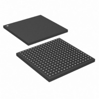
DS26518GN+ Maxim Integrated Products, DS26518GN+ Datasheet - Page 10

DS26518GN+
Manufacturer Part Number
DS26518GN+
Description
IC TXRX T1/E1/J1 8PORT 256-CSBGA
Manufacturer
Maxim Integrated Products
Type
Transceiverr
Specifications of DS26518GN+
Number Of Drivers/receivers
8/8
Protocol
T1/E1/J1
Voltage - Supply
3.135 V ~ 3.465 V
Mounting Type
Surface Mount
Package / Case
256-CSBGA
Lead Free Status / RoHS Status
Lead free / RoHS Compliant
- Current page: 10 of 286
- Download datasheet (2Mb)
2.
2.1
2.2
2.3
2.4
S 17mm x 17mm, 256-pin TE-CSBGA (1.00mm pitch)
S 3.3V supply with 5V tolerant inputs and outputs
S IEEE 1149.1 JTAG boundary scan
S Development support includes evaluation kit, driver source code, and reference designs
S Requires a single master clock (MCLK) for both E1 and T1 operation. Master clock can be 1.544MHz,
S Fully software configurable
S Short- and long-haul applications
S Ranges include 0dB to -43dB, 0dB to -30dB, 0dB to 20dB, and 0dB to -12dB for E1; 0dB to -36dB, 0dB to
S Receiver signal level indication from -2.5dB to -36dB in T1 mode and -2.5dB to -44dB in E1 mode in 2.5dB
S Software-selectable receive termination for 75:, 100:, 110:, and 120: lines
S Hitless protection switching
S Monitor application gain settings of 14dB, 20dB, 26dB, and 32dB
S G.703 receive synchronization signal mode
S Flexible transmit waveform generation
S T1 DSX-1 line build-outs
S T1 CSU line build-outs of 0dB, -7.5dB, -15dB, and -22.5dB
S E1 waveforms include G.703 waveshapes for both 75: coax and 120: twisted cables
S Analog loss-of-signal detection
S AIS generation independent of loopbacks
S Alternating ones and zeros generation
S Receiver power-down
S Transmitter power-down
S Transmit outputs and receive inputs present a high impedance to the line when no power is applied,
S Transmitter short-circuit limiter with current-limit-exceeded indication
S Transmit open-circuit-detected indication
S Backplane clocks output frequencies include 2.048MHz, 4.096MHz, 8.192MHz, and 16.384MHz
S CLKO output clock selectable from a wide range of frequencies referenced to MCLK
S 32-bit or 128-bit crystal-less jitter attenuator
S Requires only a 1.544MHz or 2.048MHz master clock or multiple thereof, for both E1 and T1 operation
S Can be placed in either the receive or transmit path or disabled
S Limit trip indication
FEATURE HIGHLIGHTS
General
Line Interface
2.048MHz, 3.088MHz, 4.096MHz, 6.176MHz, 8.192MHz, 12.352MHz, or 16.384MHz.
30dB, 0dB to 20dB, and 0dB to -12dB for T1
increments
supporting redundancy applications
Clock Synthesizers
Derived from user-selected recovered receive clock or REFCLKIO
Jitter Attenuator
10 of 286
DS26518 8-Port T1/E1/J1 Transceiver
Related parts for DS26518GN+
Image
Part Number
Description
Manufacturer
Datasheet
Request
R

Part Number:
Description:
8-port T1/e1/j1 Transceiver
Manufacturer:
Maxim Integrated Products, Inc.
Datasheet:

Part Number:
Description:
Ds26518 8-port T1/e1/j1 Transceiver
Manufacturer:
Maxim Integrated Products, Inc.

Part Number:
Description:
power light source LUXEON� Collimator
Manufacturer:
LUMILEDS [Lumileds Lighting Company]
Datasheet:

Part Number:
Description:
MAX7528KCWPMaxim Integrated Products [CMOS Dual 8-Bit Buffered Multiplying DACs]
Manufacturer:
Maxim Integrated Products
Datasheet:

Part Number:
Description:
Single +5V, fully integrated, 1.25Gbps laser diode driver.
Manufacturer:
Maxim Integrated Products
Datasheet:

Part Number:
Description:
Single +5V, fully integrated, 155Mbps laser diode driver.
Manufacturer:
Maxim Integrated Products
Datasheet:

Part Number:
Description:
VRD11/VRD10, K8 Rev F 2/3/4-Phase PWM Controllers with Integrated Dual MOSFET Drivers
Manufacturer:
Maxim Integrated Products
Datasheet:

Part Number:
Description:
Highly Integrated Level 2 SMBus Battery Chargers
Manufacturer:
Maxim Integrated Products
Datasheet:

Part Number:
Description:
Current Monitor and Accumulator with Integrated Sense Resistor; ; Temperature Range: -40°C to +85°C
Manufacturer:
Maxim Integrated Products

Part Number:
Description:
TSSOP 14/A�/RS-485 Transceivers with Integrated 100O/120O Termination Resis
Manufacturer:
Maxim Integrated Products

Part Number:
Description:
TSSOP 14/A�/RS-485 Transceivers with Integrated 100O/120O Termination Resis
Manufacturer:
Maxim Integrated Products

Part Number:
Description:
QFN 16/A�/AC-DC and DC-DC Peak-Current-Mode Converters with Integrated Step
Manufacturer:
Maxim Integrated Products

Part Number:
Description:
TDFN/A/65V, 1A, 600KHZ, SYNCHRONOUS STEP-DOWN REGULATOR WITH INTEGRATED SWI
Manufacturer:
Maxim Integrated Products

Part Number:
Description:
Integrated Temperature Controller f
Manufacturer:
Maxim Integrated Products


