ATA6622-PGQW Atmel, ATA6622-PGQW Datasheet - Page 10

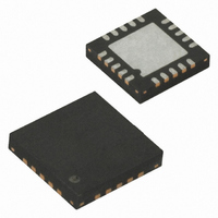
ATA6622-PGQW
Manufacturer Part Number
ATA6622-PGQW
Description
TXRX LIN BUS REG WATCHDOG 20-QFN
Manufacturer
Atmel
Type
Transceiverr
Datasheet
1.ATA6622C-PGPW.pdf
(31 pages)
Specifications of ATA6622-PGQW
Number Of Drivers/receivers
1/1
Protocol
LIN
Voltage - Supply
5 V ~ 27 V
Mounting Type
Surface Mount
Package / Case
20-QFN Exposed Pad
Processor Series
ATA6x
Core
AVR8
Data Bus Width
8 bit
Maximum Operating Temperature
+ 150 C
Mounting Style
SMD/SMT
Minimum Operating Temperature
- 40 C
Lead Free Status / RoHS Status
Lead free / RoHS Compliant
The VCC regulator is switched off. NRES and RXD are low. The internal slave termination
between the LIN pin and VS pin is disabled, only a weak pull-up current (typically 10µA)
between the LIN pin and the VS pin is present. Sleep Mode can be activated independently
from the current level on the LIN, WAKE, or KL_15 pin.
A voltage less than the LIN Pre_Wake detection VLINL at the LIN pin activates the internal LIN
receiver and switches on the internal slave termination between the LIN pin and the V
pin.
S
A falling edge at the LIN pin followed by a dominant bus level maintained for a certain time
period (> t
) and a following rising edge at pin LIN results in a remote wake-up request. The
bus
device switches from Sleep Mode to Fail-safe Mode.
The VCC regulator is activated, and the remote wake-up request is indicated by a low level at
the RXD pin to interrupt the microcontroller (see
Figure 4-5 on page
11).
EN high can be used to switch directly from Sleep/Silent to Fail-safe Mode. If EN is still high
after VCC ramp up and undervoltage reset time, the IC switches to the Normal Mode.
Figure 4-4.
Switch to Sleep Mode
Normal Mode
Sleep Mode
EN
Mode select window
TXD
t
= 3.2µs
d
NRES
VCC
Delay time sleep mode
t
= maximum 20µs
d_sleep
LIN
LIN switches directly to recessive mode
4.4
Fail-safe Mode
The device automatically switches to Fail-safe Mode at system power-up. The voltage regula-
tor is switched on (see
Figure 5-1 on page
14). The NRES output switches to low for t
= 4ms
res
and gives a reset to the microcontroller. LIN communication is switched off. The IC stays in
this mode until EN is switched to high. The IC then changes to Normal Mode. A power down of
V
(V
< 3.7V) during Silent or Sleep Mode switches the IC into Fail-safe Mode after power
Batt
S
up. A low at NRES switches into Fail-safe Mode directly. During Fail-safe Mode the TXD pin is
an output and signals the last wake-up source.
Atmel ATA6622/ATA6624/ATA6626
10
4986J–AUTO–03/11


