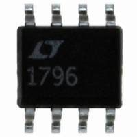
LT1796CS8 Linear Technology, LT1796CS8 Datasheet - Page 3

LT1796CS8
Manufacturer Part Number
LT1796CS8
Description
IC CAN TXRX VOLT FAULT PROT8SOIC
Manufacturer
Linear Technology
Type
Transceiverr
Datasheet
1.LT1796CS8PBF.pdf
(8 pages)
Specifications of LT1796CS8
Number Of Drivers/receivers
1/1
Protocol
CAN
Voltage - Supply
4.75 V ~ 5.25 V
Mounting Type
Surface Mount
Package / Case
8-SOIC (3.9mm Width)
Lead Free Status / RoHS Status
Contains lead / RoHS non-compliant
Available stocks
Company
Part Number
Manufacturer
Quantity
Price
Part Number:
LT1796CS8
Manufacturer:
LT/凌特
Quantity:
20 000
Company:
Part Number:
LT1796CS8#PBF
Manufacturer:
MICREL
Quantity:
235
Part Number:
LT1796CS8#PBF
Manufacturer:
LINEAR/凌特
Quantity:
20 000
Part Number:
LT1796CS8#TRPBF
Manufacturer:
LINEAR/凌特
Quantity:
20 000
SWITCHI G CHARACTERISTICS
DC ELECTRICAL CHARACTERISTICS
temperature range, otherwise specifications are at T
SYMBOL
V
V
V
I
V
V
V
I
I
temperature range. V
SYMBOL
t
F
t
t
t
t
t
t
t
t
t
SR
SR
Note 1: Absolute Maximum Ratings are those values beyond which the life
of the device may be impaired.
Note 2: Unless otherwise specified, testing done at V
SCR
RS
CC
BIT
TXDON
TXDOFF
LBON
LBOFF
RXDOFF
RXDON
RXDOFFSB
RXDONSB
WAKE
MAX
TH
OH
OL
REF
REFSC
RSSB
V
TH
+
–
PARAMETER
Differential Input Threshold Voltage
for Receiver
Receiver Input Hysteresis
Receiver Output High Voltage
Receiver Output Low Voltage
Receiver Short-Circuit Current
Reference Output Voltage
Reference Output Short-Circuit Current
R
R
Supply Current Dominant
PARAMETER
Minimum Bit Time
Maximum Data Rate
Driver Input to Bus Active
Driver Input to Bus Inactive
Loopback Delay Active
Loopback Delay Inactive
Receiver Delay Off
Receiver Delay On
Receiver Delay Off, Standby
Receiver Delay On, Standby
Wake-Up Delay from Standby
Positive Slew Rate
Negative Slew Rate
S
S
U
Pin Standby Threshold
Input Current
RS
= 0V unless otherwise noted. (Note 2)
Recessive
Standby
CC
= 5V, T
A
CONDITIONS
V
V
– 7V < V
V
V
0V < V
– 100 A < I
0 < V
V
V
V
R
No Load, V
R
R
CONDITIONS
(Note 3)
(Note 3)
Figures 1, 2
Figures 1, 2
Figures 1, 3
Figures 1, 3
Figures 1, 4
Figures 1, 4
V
V
Figures 1, 5
R
R
R
R
RS
RS
CC
CC
CC
RS
RS
S
L
L
RS
RS
S
S
S
S
= 25 C. V
A
= 47k
= 47k
= 47k, V
= 60 , V
= 60 , V
= 0k
= 0k
= 25 C.
= 5V, – 7V < V
= 5V, V
= 0V, V
= 4V, Figures 1, 4
= 4V, Figures 1, 4
= 0V, – 7V < V
= 4.75V, I
= 4.75V, I
= 5V
REF
O
The
CM
< V
< V
RS
REF
CC
< 12V
CC
CC
CC
CC
RS
RS
CC
= 0V, V
O
O
The
= 5V
= 5V
= 5V
denotes the specifications which apply over the full operating
, V
< 100 A
= 0V, V
= 5V, V
= – 400 A, V
= 1.6mA, V
= 4.75V to 5.25V, V
CC
CM
CM
Note 3: Bit time and data rate specifications are guaranteed by driver and
receiver delay time measurements.
= 5.25V
TXD
denotes the specifications which apply over the full operating
< 12V
< 12V
TXD
CC
= 0V, V
= 5.25V
= 5V, V
ID
ID
= 900mV
R
R
R
R
= 500mV
S
S
S
S
CC
= 47k
= 47k
= 0k
= 0k
CC
= 5.25V
= 5.25V
RS
= 0V unless otherwise noted.
– 270
MIN
– 20
– 90
MIN
125
0.5
0.5
2.5
2.25
3
7
5
2
5
2
– 200
0.15
TYP
– 60
TYP
300
350
500
600
400
300
3.6
2.5
2.8
0.1
4.3
3.8
0.8
0.6
1.5
1.5
70
20
12
36
1
1
7
5
– 140
1000
1000
1500
MAX
MAX
– 40
500
600
600
0.9
0.9
0.4
2.7
1.5
1.5
85
20
10
15
65
30
65
15
4
7
7
8
3
4
4
LT1796
UNITS
UNITS
3
kbps
V/ s
V/ s
V/ s
V/ s
1796f
mV
mA
mA
mA
mA
mA
ns
ns
ns
ns
ns
ns
V
V
V
V
V
V
A
A
A
s
s
s
s
s
s


