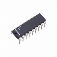
LTC1384CN Linear Technology, LTC1384CN Datasheet - Page 5

LTC1384CN
Manufacturer Part Number
LTC1384CN
Description
IC TXRX 5V RS232 LOW PWR 18-DIP
Manufacturer
Linear Technology
Type
Transceiverr
Datasheet
1.LTC1384CNPBF.pdf
(8 pages)
Specifications of LTC1384CN
Number Of Drivers/receivers
2/2
Protocol
RS232
Voltage - Supply
4.5 V ~ 5 V
Mounting Type
Through Hole
Package / Case
18-DIP (0.300", 7.62mm)
Lead Free Status / RoHS Status
Contains lead / RoHS non-compliant
Available stocks
Company
Part Number
Manufacturer
Quantity
Price
Part Number:
LTC1384CN
Manufacturer:
LT/凌特
Quantity:
20 000
Company:
Part Number:
LTC1384CN#PBF
Manufacturer:
LTC
Quantity:
209
SWITCHI G TI E WAVEFOR S
PI FU CTIO S
V
with a 0.1µF ceramic capacitor.
GND: Ground Pin.
ON/OFF: TTL/CMOS Compatible Shutdown Pin. A logic
low puts the device in the Shutdown mode independent of
the RX EN pin. The supply current of the device drops to
35µA (two receivers alive) and both driver outputs are
forced into three-state.
RX EN: TTL/CMOS Compatible Receiver Enable Pin. A
logic high forces the receiver outputs into three-state. A
logic low enables the receiver outputs.
V
2V. This pin requires an external capacitor C = 0.1µF for
charge storage. The capacitor may be tied to ground or
V
a common capacitor. For large numbers of devices, in-
creasing the size of the shared common storage capaci-
tors is recommended to reduce ripple.
V
– 2V). This pin requires an external capacitor C = 0.1µF for
charge storage.
OUTPUT
CC
CC
DRIVER
DRIVER
+
–
INPUT
: Positive Supply Output (RS232 Drivers). V
: Negative Supply Output (RS232 Drivers). V
U
: 5V Input Supply Pin. This pin should be decoupled
. With multiple devices, the V
t
Figure 1. Driver Propagation Delay Timing
LHD
U
1.4V
U
0V
U
W
+
and V
1.4V
–
pins may share
t
HLD
W
–
+
≅ – (2V
≅ 2V
0V
LTC1384 • F01
V
V
CC
V
0V
CC
+
–
CC
–
C1
pins require two external capacitors C = 0.1µF: one from
C1
charge pump efficiency, the capacitor’s effective series
resistance should be less than 2Ω.
TR IN: RS232 Driver Input Pins. Inputs are TTL/CMOS
compatible. The inputs of unused drivers can be left
unconnected since 300k input pull-up resistors to V
included on chip. To minimize power consumption, the
internal driver pull-up resistors are disconnected from V
in the Shutdown mode.
TR OUT: Driver Outputs at RS232 Voltage Levels. Outputs
are in a high impedance state when in the Shutdown or V
= 0V. The driver outputs are protected against ESD to
±10kV for human body model discharges.
RX IN: Receiver Inputs. These pins can be forced to ±25V
without damage. The receiver inputs are protected against
ESD to ±10kV for human body model discharges. Each
receiver provides 0.4V of hysteresis for noise immunity.
RX OUT: Receiver Outputs with TTL/CMOS Voltage Lev-
els. A logic high at RX EN puts the outputs into three-state.
OUTPUT
INPUT
+
+
, C1
RX
RX
to C1
–
t
Figure 2. Receiver Propagation Delay Timing
LHR
, C2
–
and another from C2
+
, C2
1.7V
0.8V
–
: Commutating Capacitor Inputs. These
+
to C2
1.3V
LTC1384
–
. To maintain
t
HLR
2.4V
LTC1384 • F02
CC
1384fa
V
0V
V
0V
5
CC
CC
are
CC
CC


