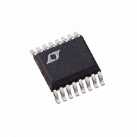
LT6300IGN#TRPBF Linear Technology, LT6300IGN#TRPBF Datasheet - Page 10

LT6300IGN#TRPBF
Manufacturer Part Number
LT6300IGN#TRPBF
Description
IC XDSL LINE DRIVER 16-SSOP
Manufacturer
Linear Technology
Type
Line Driver, Transmitterr
Datasheet
1.LT6300CGNPBF.pdf
(16 pages)
Specifications of LT6300IGN#TRPBF
Number Of Drivers/receivers
2/0
Protocol
xDSL
Voltage - Supply
5 V ~ 12 V
Mounting Type
Surface Mount
Package / Case
16-SSOP
Lead Free Status / RoHS Status
Lead free / RoHS Compliant
Available stocks
Company
Part Number
Manufacturer
Quantity
Price
APPLICATIO S I FOR ATIO
LT6300
which looks very much like noise, it is easiest to use the
RMS values of voltages and currents for estimating the
driver power dissipation. The voltage and current levels
shown for this example are for a full-rate ADSL signal
driving 20dBm or 100mW
telephone line and assuming a 0.5dBm insertion loss in
the transformer. The quiescent current for the LT6300 is
set to 10mA per amplifier.
The power dissipated in the LT6300 is a combination of the
quiescent power and the output stage power when driving
a signal. The two amplifiers are configured to place a
differential signal on to the line. The Class AB output stage
in each amplifier will simultaneously dissipate power in
the upper power transistor of one amplifier, while sourc-
ing current, and the lower power transistor of the other
amplifier, while sinking current. The total device power
dissipation is then:
With no signal being placed on the line and the amplifier
biased for 10mA per amplifier supply current, the quies-
cent driver power dissipation is:
This can be reduced in many applications by operating
with a lower quiescent current value.
10
P
P
P
D
D
DQ
= P
= (V
= 24V • 20mA = 480mW
I
LOAD
QUIESCENT
+
– V
+ (V
–
) • I
–
U
+ P
Q
– V
+ (V
Q(UPPER)
OUTBRMS
U
+
25
20
15
10
RMS
5
0
–240
– V
OUTARMS
of power on to the 100
–200
+ P
) • I
W
Q(LOWER)
LOAD
–160
) •
–120
U
–80
Figure 7. I
–40
I
LOAD
0
Q
(mA)
vs I
When driving a load, a large percentage of the amplifier
quiescent current is diverted to the output stage and
becomes part of the load current. Figure 7 illustrates the
total amount of biasing current flowing between the + and
– power supplies through the amplifiers as a function of
load current. As much as 60% of the quiescent no load
operating current is diverted to the load.
At full power to the line the driver power dissipation is:
The junction temperature of the driver must be kept less
than the thermal shutdown temperature when processing
a signal. The junction temperature is determined from the
following expression:
LT6300 to the ambient air, which can be minimized by
heat-spreading PCB metal and airflow through the enclo-
sure as required. For the example given, assuming a
maximum ambient temperature of 50 C and keeping the
junction temperature of the LT6300 to 150 C maximum,
the maximum thermal resistance from junction to ambient
required is:
JA
40
LOAD
P
P
T
J
D(FULL)
D(FULL)
is the thermal resistance from the junction of the
JA MAX
= T
(
80
AMBIENT
120
)
= 24V • 8mA + (12V – 2V
= 192mW + 570mW + 570mW = 1.332W
+ [|–12V – (– 2V
150
160
( C) + P
1 332
.
C
200
–
6300 F07
50
W
D(FULL)
240
C
RMS
75 1
(W) •
)|] • 57mA
.
RMS
C W
/
JA
) • 57mA
( C/W)
RMS
RMS


