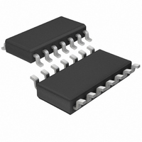
LTC491IS#TR Linear Technology, LTC491IS#TR Datasheet - Page 3

LTC491IS#TR
Manufacturer Part Number
LTC491IS#TR
Description
IC TXRX RS485 LOW POWER 14-SOIC
Manufacturer
Linear Technology
Type
Transceiverr
Datasheet
1.LTC491CNPBF.pdf
(12 pages)
Specifications of LTC491IS#TR
Number Of Drivers/receivers
1/1
Protocol
RS422, RS485
Voltage - Supply
4.75 V ~ 5.25 V
Mounting Type
Surface Mount
Package / Case
14-SOIC (3.9mm Width), 14-SOL
Lead Free Status / RoHS Status
Contains lead / RoHS non-compliant
Available stocks
Company
Part Number
Manufacturer
Quantity
Price
PI FU CTIO S
S
temperature range, otherwise specifications are at T
SYMBOL
t
t
t
t
t
t
t
t
t
t
t
t
t
t
t
Note 1: Absolute Maximum Ratings are those values beyond which the life
of the device may be impaired.
Note 2: All currents into device pins are positive; all currents out of device
pins are negative. All voltages are referenced to device ground unless
otherwise specified.
NC (Pin 1): Not Connected.
R (Pin 2): Receiver Output. If the receiver output is enabled
(REB low), then if A > B by 200mV, R will be high. If A < B
by 200mV, then R will be low.
REB (Pin 3): Receiver Output Enable. A low enables the
receiver output, R. A high input forces the receiver output
into a high impedance state.
DE (Pin 4): Driver Output Enable. A high on DE enables the
driver outputs, Y and Z. A low input forces the driver
outputs into a high impedance state.
D (Pin 5): Driver Input. If the driver outputs are enabled
(DE high), then a low on D forces the driver outputs Y low
and Z high. A high on D will force Y high and Z low.
PLH
PHL
SKEW
r
ZH
ZL
LZ
HZ
PLH
PHL
SKD
ZL
ZH
LZ
HZ
, t
WITCHI
f
U
PARAMETER
Driver Input to Output
Driver Input to Output
Driver Output to Output
Driver Rise or Fall Time
Driver Enable to Output High
Driver Enable to Output Low
Driver Disable Time From Low
Driver Disable Time From High
Receiver Input to Output
Receiver Input to Output
Receiver Enable to Output Low
Receiver Enable to Output High
Receiver Disable From Low
Receiver Disable From High
U
t
PLH
U
– t
G C
PHL
U
Differential Receiver Skew
HARA TERISTICS
C
A
= 25 C. V
The
(Figures 2, 5)
CONDITIONS
R
C
C
C
C
R
(Figures 2, 7)
C
C
C
C
L
L
L
L
L
L
L
L
DIFF
DIFF
= 100pF (Figures 4, 6) S2 Closed
= 100pF (Figures 4, 6) S1 Closed
= 15pF (Figures 4, 6) S1 Closed
= 15pF (Figures 4, 6) S2 Closed
= 15pF (Figures 3, 8) S1 Closed
= 15pF (Figures 3, 8) S2 Closed
= 15pF (Figures 3, 8) S1 Closed
= 15pF (Figures 3, 8) S2 Closed
CC
denotes the specifications which apply over the full operating
= 54 , C
= 54 , C
= 5V 5%
GND (Pin 6): Ground Connection.
GND (Pin 7): Ground Connection.
NC (Pin 8): Not Connected.
Y (Pin 9): Driver Output.
Z (Pin 10): Driver Output.
B (Pin 11): Receiver Input.
A (Pin 12): Receiver Input.
NC (Pin 13): Not Connected.
V
Note 3: All typicals are given for V
CC
L1
L1
(Pin 14): Positive Supply; 4.75V V
= C
= C
L2
L2
= 100pF
= 100pF
CC
= 5V and temperature = 25 C.
MIN
10
10
40
40
5
TYP
30
30
15
40
40
40
40
70
70
13
20
20
20
20
5
CC
MAX
150
150
50
50
25
70
70
70
70
50
50
50
50
LTC491
5.25V.
UNITS
3
491fa
ns
ns
ns
ns
ns
ns
ns
ns
ns
ns
ns
ns
ns
ns
ns


