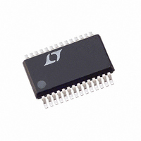
LT1330CG Linear Technology, LT1330CG Datasheet

LT1330CG
Specifications of LT1330CG
Available stocks
Related parts for LT1330CG
LT1330CG Summary of contents
Page 1
... The LT1330 operates to 120kbaud even driving high capacitive loads. During shutdown, driver and receiver outputs are at a high impedance state allowing devices to be paralleled. L, LT, LTC and LTM are registered trademarks of Linear Technology Corporation. TransZorb is a registered trademark of General Instrments, GSI. – 28 ...
Page 2
... L DR3 OUT RX5 IN (LOW-Q) ON/OFF 3V V 28-LEAD PLASTIC SSOP Consult factory for Military grade parts. PART MARKING PACKAGE DESCRIPTION LT1330CG 28-Lead Plastic SSOP LT1330CNW 28-Lead (Wide) PDIP LT1330CSW 28-Lead (Wide) Plastic SO http://www.linear.com/leadfree/ http://www.linear.com/tapeandreel/ l The denotes the specifi cations which apply over the full operating ...
Page 3
ELECTRICAL CHARACTERISTICS temperature range (0°C ≤ T ≤ 70°C for commercial grade). (Note 2) A PARAMETER CONDITIONS Supply Current When OFF (V ) Shutdown (Note 5) CC Driver Disable Supply Rise Time 0.2μ Shutdown ...
Page 4
LT1330 ELECTRICAL CHARACTERISTICS temperature range (0°C ≤ T ≤ 70°C for commercial grade). A Note 1: Stresses beyond those listed under Absolute Maximum Ratings may cause permanent damage to the device. Exposure to any Absolute Maximum Rating condition for extended ...
Page 5
TYPICAL PERFORMANCE CHARACTERISTICS ON/OFF Thresholds 3.0 2.5 2.0 ON THRESHOLD 1.5 1.0 OFF THRESHOLD 0.5 0 –55 – 100 TEMPERATURE (°C) 1330 G07 Driver Short-Circuit Current – ...
Page 6
LT1330 PIN FUNCTIONS Input Supply Pin. This pin should be decoupled CC with a 0.1μF ceramic capacitor close to the package pin. Insuffi cient supply bypassing can result in low output drive levels and erratic charge pump ...
Page 7
... The driver disable mode turns off the charge pump and RS232 drivers, but keeps all fi ve receivers active. Power consumption in driver disable mode is 3mA from V Burst Mode is a registered trademark of Linear Technology Corporation. LT1330 ESD Test Circuit – ...
Page 8
LT1330 PACKAGE DESCRIPTION 0.150 ± 0.005 0.600 – 0.625 (15.240 – 15.875) (3.810 ± 0.127) 0.015 (0.381) MIN 0.009 – 0.015 (0.229 – 0.381) +0.035 0.625 –0.015 0.125 0.035 – 0.080 ( ) +0.889 (3.175) (0.889 – 2.032) 15.87 –0.381 ...
Page 9
... FLASH SHALL NOT EXCEED 0.010" (0.254mm) PER SIDE Information furnished by Linear Technology Corporation is believed to be accurate and reliable. However, no responsibility is assumed for its use. Linear Technology Corporation makes no representation that the interconnection of its circuits as described herein will not infringe on existing patent rights. ...
Page 10
... LOGIC “0” RX1 OUT 24 DRIVER LOGIC “0” RX2 OUT 22 RX3 OUT 21 MOUSE DATA RX4 OUT 20 DRIVER LOGIC “1” RX5 OUT (LOW-Q) 18 GND 17 DRIVER DISABLE 16 15 1330 TA03 LT 0209 REV B • PRINTED IN USA © LINEAR TECHNOLOGY CORPORATION 1992 1330fb ...


