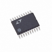
LT1739CFE Linear Technology, LT1739CFE Datasheet

LT1739CFE
Specifications of LT1739CFE
Available stocks
Related parts for LT1739CFE
LT1739CFE Summary of contents
Page 1
... DFN package or a 20-lead TSSOP for maximum port density in central office line driver applications. For a dual version of the LT1739, see the LT6301 data sheet. , LTC and LT are registered trademarks of Linear Technology Corporation. 1:2* 100 1739 TA01 *COILCRAFT X8390-A OR EQUIVALENT ...
Page 2
... Junction Temperature FE Package ....................................................... 150 C UE Package ...................................................... 125 C Storage Temperature Range FE Package ....................................... – 150 C UE Package ...................................... – 125 C Lead Temperature (Soldering, 10 sec).................. 300 ORDER PART NUMBER LT1739CFE –IN A LT1739IFE +IN A SHDN SHDNREF +IN B –IN B 12-LEAD (4mm 3mm) PLASTIC DFN T = 125 C, JMAX ...
Page 3
ELECTRICAL CHARACTERISTICS The denotes the specifications which apply over the full specified temperature range, otherwise specifications are 0V, pulse tested 12V SYMBOL PARAMETER R Input Resistance IN C Input Capacitance IN ...
Page 4
LT1739 W U TYPICAL PERFOR A CE CHARACTERISTICS Supply Current vs Ambient Temperature 12V 24.9k TO SHDN BIAS SHDNREF –50 –30 ...
Page 5
W U TYPICAL PERFOR A CE CHARACTERISTICS CMRR vs Frequency 100 12V 10mA PER AMPLIFIER 0 100 ...
Page 6
LT1739 W U TYPICAL PERFOR A CE CHARACTERISTICS Differential Harmonic Distortion vs Supply Current –40 –45 –50 – 1MHz, HD3 –60 – 100kHz, HD2 –70 – 100kHz, HD3 – 1MHz, HD2 –85 ...
Page 7
U U APPLICATIO S I FOR ATIO The LT1739 is a high speed, 200MHz gain bandwidth product, dual voltage feedback amplifier with high output current drive capability, 500mA source and sink. The LT1739 is ideal for use as a line ...
Page 8
... F04 Figure 4. Providing Logic Input Control of Operating Current Linear Technology for assistance in implementing a single supply design with operating current control. These modes can be useful for overall system power manage- ment when full power transmissions are not necessary. Shutdown and Recovery ...
Page 9
U U APPLICATIO S I FOR ATIO the design of the PCB and card enclosure to take measures to spread the heat developed in the driver away to the ambient environment to prevent thermal shutdown (which occurs when the junction ...
Page 10
LT1739 U U APPLICATIO S I FOR ATIO –240 –200 –160 –120 –80 – (mA) LOAD Figure LOAD At full power to the line the driver ...
Page 11
U U APPLICATIO S I FOR ATIO When PCB cards containing multiple ports are inserted into a rack in an enclosed cabinet often necessary to provide airflow through the cabinet and over the cards. As STILL AIR PACKAGE ...
Page 12
LT1739 U U APPLICATIO S I FOR ATIO Layout and Passive Components With a gain bandwidth product of 200MHz the LT1739 requires attention to detail in order to extract maximum performance. Use a ground plane, short lead lengths and a ...
Page 13
U U APPLICATIO S I FOR ATIO In differential driver applications, as shown on the first page of this data sheet recommended that the gain setting resistor be comprised of two equal value resistors connected to a good ...
Page 14
... Extra gain may be required in the receive channel to compensate completely separate receive path may be implemented through a separate line coupling transformer. A demo board, DC306A-C, is available for the LT1739CFE. This demo board is a complete line driver with an LT1361 receiver included. It allows the evaluation of both standard and active termination approaches ...
Page 15
U U APPLICATIO S I FOR ATIO Using DC blocking capacitors, as shown in Figure 16 couple the signal to the transformer eliminates the possibility for DC current to flow under any conditions. These capacitors should be sized ...
Page 16
... Figure 17. LT1739, LT1361 ADSL Demo Board (DC306A- 15.4 1/ 2010 U2A 18 2 LT1739CFE 5 – COILCRAFT EE X8504-A R4 2.49k C18 OPT R6 1206 2.49k 15.4 1/2W + 2010 U2B 13 LT1739CFE 6 – 19 R10 ON/OFF JP3 R11 + 1.6k 7 U4B LT1541CS8 R14 – 4 1.6k ADJ FIXED R19 JP4 R17 U4A 1 Q1 21.5k LT1541CS8 FMMT3904 1 – ...
Page 17
PLIFIED SCHE ATIC + V –IN – V (one amplifier shown) Q9 Q10 Q12 Q11 LT1739 Q13 Q17 C1 Q14 +IN OUT Q15 C2 Q18 Q16 1739 SS ...
Page 18
LT1739 PACKAGE DESCRIPTIO 6.60 0.10 4.50 0.10 SEE NOTE 4 RECOMMENDED SOLDER PAD LAYOUT 4.30 – 4.50* (.169 – .177) 0.45 – 0.75 0.09 – 0.20 (.018 – .030) (.0036 – .0079) NOTE: 1. CONTROLLING DIMENSION: MILLIMETERS 2. DIMENSIONS ARE ...
Page 19
... MOLD FLASH. MOLD FLASH, IF PRESENT, SHALL NOT EXCEED 0.15mm ON ANY SIDE 4. EXPOSED PAD SHALL BE SOLDER PLATED Information furnished by Linear Technology Corporation is believed to be accurate and reliable. However, no responsibility is assumed for its use. Linear Technology Corporation makes no represen- tation that the interconnection of its circuits as described herein will not infringe on existing patent rights. U ...
Page 20
... Low Noise, Low Power Differential Receiver, 4mA/Amplifier 12V Operation, 7mA/Amplifier, ADSL Modem Line Driver 12V Operation, MSOP Package, ADSL Modem Line Driver ADSL CO Driver in SSOP Package 100 LINE 1739 F17 , 1739fas, sn1739 LT/TP 0602 1.5K REV A • PRINTED IN THE USA LINEAR TECHNOLOGY CORPORATION 2001 ...


