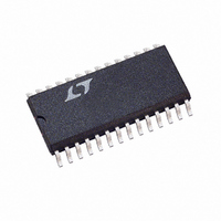
LTC1535CSW#PBF Linear Technology, LTC1535CSW#PBF Datasheet - Page 3

LTC1535CSW#PBF
Manufacturer Part Number
LTC1535CSW#PBF
Description
IC TRANSCEIVER RS485 ISO 28SOIC
Manufacturer
Linear Technology
Type
Transceiverr
Specifications of LTC1535CSW#PBF
Number Of Drivers/receivers
1/1
Protocol
RS485
Voltage - Supply
4.5 V ~ 5.5 V
Mounting Type
Surface Mount
Package / Case
28-SOIC (7.5mm Width)
Device Type
Differential
Interface Type
RS422, RS485
No. Of Drivers
1
Supply Voltage Range
4.5V To 7.5V
Driver Case Style
SOIC
No. Of Pins
28
Operating Temperature Range
0°C To +70°C
Svhc
No
Rohs Compliant
Yes
Lead Free Status / RoHS Status
Lead free / RoHS Compliant
Available stocks
Company
Part Number
Manufacturer
Quantity
Price
ELECTRICAL CHARACTERISTICS
temperature range, otherwise specifications are at T
SYMBOL
V
V
V
I
V
V
f
R
R
I
I
V
V
V
SWITCHI G CHARACTERISTICS
temperature range, otherwise specifications are at T
SYMBOL
t
f
t
t
t
t
t
t
t
t
t
t
t
t
t
t
t
t
OZ
SW
REL
REH
SJ
MAX
PLH
PHL
r
ZH
ZL
LZ
HZ
PLH
PHL
PLH
PHL
r
LZ
HZ
START
TOF
IOC
OH
OL
OH2
OL2
UVL
UVH
ISO
, t
, t
SWH
SWL
f
f
PARAMETER
Receiver Input Open Circuit Voltage
RO Output High Voltage
RO Output Low Voltage
Driver Output Leakage
RO2 Output High Voltage
RO2 Output Low Voltage
DC Converter Frequency
DC Converter Impedance High
DC Converter Impedance Low
RE Output Low Current
RE Output High Current
Undervoltage Low Threshold
Undervoltage High Threshold
Isolation Voltage
PARAMETER
Data Sample Jitter
Max Baud Rate
Driver Input to Output
Driver Input to Output
Driver Rise or Fall Time
Driver Enable to Output
Driver Enable to Output
Driver Disable to Output
Driver Disable to Output
Receiver Input to RO
Receiver Input to RO
Receiver Input to RO2
Receiver Input to RO2
Receiver Rise or Fall Time
Receiver Disable to Output
Receiver Disable to Output
Initial Start-Up Time
Data Time-Out Fault
ST1, ST2 Duty Cycle
U
CONDITIONS
I
I
Driver Disabled (DE = 0)
I
I
RE Sink Current, Fault = 0
RE Source Current, Fault = 1
RE Fault = 1, (Note 5)
RE Fault = 0, (Note 5)
1 Minute, (Note 6)
1 Second
CONDITIONS
Figure 8, (Note 7)
Jitter = 10% Max, SLO = 1, (Note 8)
DE = 1, SLO = 1, Figure 4, Figure 6
DE = 1, SLO = 0, Figure 4, Figure 6
DE = 1, SLO = 1, Figure 4, Figure 6
DE = 1, SLO = 0, Figure 4, Figure 6
DE = 1, SLO = 1, Figure 4, Figure 6
DE = 1, SLO = 0, V
DI = 1, SLO = 1, Figure 5, Figure 7
DI = 0, SLO = 1, Figure 5, Figure 7
DI = 0, SLO = 1, Figure 5, Figure 7
DI = 1, SLO = 1, Figure 5, Figure 7
RE = 0, Figure 3, Figure 8
RE = 0, Figure 3, Figure 8
RE = 0, Figure 3, Figure 8
RE = 0, Figure 3, Figure 8
RE = 0, Figure 3, Figure 8
Figure 3, Figure 9
Figure 3, Figure 9
(Note 9)
(Note 9)
0 C T
– 40 C T
RO
RO
RO2
RO2
A
A
= 25 C. V
= 25 C. V
= – 4mA, V
= 4mA, V
= – 4mA, V
= 4mA, V
A
The
The
A
70 C
CC
CC
85 C
CC
CC
CC
CC
= 4.5V
denotes the specifications which apply over the full operating
= 4.5V
denotes the specifications which apply over the full operating
= 4.5V
= 5V, V
= 5V, V
= 4.5V
CC
= V
CC2
CC2
CC2
= 4.5V
= 5V unless otherwise noted.
= 5V, R = 27 (RS485) unless otherwise noted.
2500
3000
3.70
4.05
MIN
– 40
MIN
290
250
150
3.7
3.7
80
1300
1300
1000
1000
1200
1200
4.00
4.20
TYP
– 50
TYP
420
100
250
410
600
600
500
700
700
600
600
3.4
4.0
0.4
3.9
0.4
2.5
20
30
30
20
30
30
1
4
LTC1535
1560
1560
1000
1400
1400
1300
1300
MAX
4.25
4.40
MAX
– 80
590
130
285
855
855
100
855
855
0.8
0.8
56
57
6
5
UNITS
UNITS
V
V
1535fa
3
RMS
RMS
kHz
kBd
ns
ns
ns
ns
ns
ns
ns
ns
ns
ns
ns
ns
ns
ns
ns
ns
ns
ns
ns
ns
%
%
V
V
V
A
V
V
A
A
V
V


