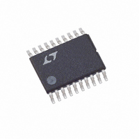
LT1794CFE#TRPBF Linear Technology, LT1794CFE#TRPBF Datasheet - Page 10

LT1794CFE#TRPBF
Manufacturer Part Number
LT1794CFE#TRPBF
Description
IC AMP XDSL LINE DRIVER 20TSSOP
Manufacturer
Linear Technology
Type
Line Driver, Transmitterr
Datasheet
1.LT1794CSWPBF.pdf
(20 pages)
Specifications of LT1794CFE#TRPBF
Number Of Drivers/receivers
2/0
Protocol
xDSL
Voltage - Supply
18V
Mounting Type
Surface Mount
Package / Case
20-TSSOP Exposed Pad, 20-eTSSOP, 20-HTSSOP
Lead Free Status / RoHS Status
Lead free / RoHS Compliant
Available stocks
Company
Part Number
Manufacturer
Quantity
Price
APPLICATIO S I FOR ATIO
LT1794
Power Dissipation and Heat Management
xDSL applications require the line driver to dissipate a
significant amount of power and heat compared to other
components in the system. The large peak to RMS varia-
tions of DMT and CAP ADSL signals require high supply
voltages to prevent clipping, and the use of a step-up
transformer to couple the signal to the telephone line can
require high peak current levels. These requirements
result in the driver package having to dissipate on the
order of 1W. Several multiport cards inserted into a rack
in an enclosed central office box can add up to many,
many watts of power dissipation in an elevated ambient
temperature environment. The LT1794 has built-in ther-
mal shutdown circuitry that will protect the amplifiers if
operated at excessive temperatures, however data trans-
missions will be seriously impaired. It is important in the
design of the PCB and card enclosure to take measures to
spread the heat developed in the driver away to the
ambient environment to prevent thermal shutdown (which
occurs when the junction temperature of the LT1794
exceeds 165 C).
10
1000pF
U
+IN
–IN
U
110
110
20mA DC
W
Figure 6. Estimating Line Driver Power Dissipation
–
+
+
–
A
B
–12V
1k
1k
12V
I
LOAD
SHDN
SHDNREF
U
24.9k – SETS I
–2V
2V
= 57mA
RMS
RMS
17.4
17.4
RMS
Q
PER AMPLIFIER = 10mA
1:1.7
1794 F06
Estimating Line Driver Power Dissipation
Figure 6 is a typical ADSL application shown for the
purpose of estimating the power dissipation in the line
driver. Due to the complex nature of the DMT signal,
which looks very much like noise, it is easiest to use the
RMS values of voltages and currents for estimating the
driver power dissipation. The voltage and current levels
shown for this example are for a full-rate ADSL signal
driving 20dBm or 100mW
telephone line and assuming a 0.5dBm insertion loss in
the transformer. The quiescent current for the LT1794 is
set to 10mA per amplifier.
The power dissipated in the LT1794 is a combination of the
quiescent power and the output stage power when driving
a signal. The two amplifiers are configured to place a
differential signal on to the line. The Class AB output stage
in each amplifier will simultaneously dissipate power in
the upper power transistor of one amplifier, while sourc-
ing current, and the lower power transistor of the other
amplifier, while sinking current. The total device power
dissipation is then:
P
P
D
D
= P
= (V
I
LOAD
QUIESCENT
+
– V
+ (V
–
) • I
–
+ P
Q
– V
100
+ (V
Q(UPPER)
OUTBRMS
+
RMS
– V
OUTARMS
of power on to the 100
+ P
) • I
3.16V
Q(LOWER)
LOAD
RMS
) •


