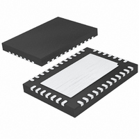
LTC2847CUHF Linear Technology, LTC2847CUHF Datasheet - Page 15

LTC2847CUHF
Manufacturer Part Number
LTC2847CUHF
Description
IC TXRX MULTIPROTOCOL 38-QFN
Manufacturer
Linear Technology
Type
Transceiverr
Datasheet
1.LTC2847IUHFPBF.pdf
(20 pages)
Specifications of LTC2847CUHF
Number Of Drivers/receivers
3/3
Protocol
Multiprotocol
Voltage - Supply
5V
Mounting Type
Surface Mount
Package / Case
38-QFN
Lead Free Status / RoHS Status
Contains lead / RoHS non-compliant
Available stocks
Company
Part Number
Manufacturer
Quantity
Price
Company:
Part Number:
LTC2847CUHF
Manufacturer:
LT
Quantity:
10 000
Part Number:
LTC2847CUHF
Manufacturer:
LINEAR/凌特
Quantity:
20 000
Part Number:
LTC2847CUHF#TRPBF
Manufacturer:
LINEAR/凌特
Quantity:
20 000
DTE vs DCE Operation
The DCE/DTE pin acts as an enable for Driver 3/Receiver 1
in the LTC2847, and Driver 3/Receiver 1 in the LTC2845.
The LTC2847/LTC2845 can be configured for either DTE
or DCE operation in one of two ways: a dedicated DTE or
DCE port with a connector of appropriate gender or a port
with one connector that can be configured for DTE or DCE
operation by rerouting the signals to the LTC2847/LTC2845
using a dedicated DTE cable or dedicated DCE cable.
A dedicated DTE port using a DB-25 male connector is
shown in Figure 29. The interface mode is selected by logic
outputs from the controller or from jumpers to either V
or GND on the mode select pins. A dedicated DCE port
using a DB-25 female connector is shown in Figure 30.
A port with one DB-25 connector, that can be configured
for either DTE or DCE operation is shown in Figure 31. The
configuration requires separate cables for proper signal
routing in DTE or DCE operation. For example, in DTE
mode, the TXD signal is routed to Pins 2 and 14 via the
LTC2847’s Driver 1. In DCE mode, Driver 1 now routes the
RXD signal to Pins 2 and 14.
Power Dissipation Calculations
The LTC2847 takes in 5V V
produced from V
approximately 80% and 70% efficiency respectively. Cur-
rent drawn internally from V
into a higher I
ing to the equation:
P
receiver termination on the far end of the cable while N
is the number of drivers. Conversely, current from the
far end drivers dissipate power N
receiver termination where N
ers.
LTC2847 Power Dissipation
Consider an LTC2847 in X.21, DCE mode (three V.11
drivers and two V.11 receivers). From the Electrical Char-
acteristics Table, I
100mA. Each receiver termination is 100
TYPICAL APPLICATIO S
RT
P
DISS(2847)
refers to the power dissipated by each driver in a
CC
= V
. The LTC2847 dissipates power accord-
CC
CC
CC
• I
at no load = 14mA, I
with an internal charge pump at
CC
– N
DD
CC
D
R
• P
is the number of receiv-
. V
or V
R
U
RT
DD
• P
EE
+ N
and V
RT
translates directly
R
in the internal
CC
• P
EE
at full load =
RT
are in turn
(R
RT
) and
(1)
IN
D
current going into each receiver termination = (100mA –
14mA)/3 = 28.7mA (I
From Equation (2), P
DC power dissipation P
82.4mW + 2 • 82.4mW = 418mW.
Consider the above example running at a baud rate of
10MBd. From the Typical Characteristic for “V.11 Mode
I
increases with baud rate due to driver transient dissipa-
tion. From Equation (1), AC power dissipation P
= 5V • 160mA –3 • 82.4mW + 2 • 82.4mW = 718mW.
LTC2845 Power Dissipation
If a LTC2845 is used to form a complete DCE port with the
LTC2847, it will be running in the X.21 mode (three V.11
drivers and two V.10 drivers, two V.11 receivers and two
V.10 receivers, all with internal 30k termination). In addi-
tion to V
LTC2847. Negligible power is dissipated in the large
internal receiver termination of the LTC2845 so the N
P
is modified as follows:
Since power is drawn from the supplies of the LTC2847
(V
dissipates extra power to source P
From the LTC2845 Electrical Characteristics Table, for
V
I
I
I
I
I
I
CC
CC
EE
EE
DD
DD
CC
RT
CC
P
DD
at no load
at full load with both V.10 drivers low
P
P
at no load
at full load with all drivers high
at no load
at full load
RT
term of Equation (1) can be omitted. Thus Equation (1)
DISS(2845)
DISS1(2847)
vs Data Rate,” the I
= 5V, V
and V
= (I
CC
RT
EE
, it uses the V
DD
)
2
) at less than 100% efficiency, the LTC2847
• R
= (V
+ (V
= 8V and V
= 125% • (V
= 25% • (V
(V
RT
CC
EE
EE
RT
• I
• I
RT
• I
= 82.4mW and from Equation (1),
EE
CC
).
EE
DISS(2847)
) – N
) + (V
) – P
EE
CC
DD
DD
DD
= – 5.5V:
• I
at 10MBd is 160mA. I
and V
D
• I
DISS(2845)
DD
DD
• P
DD
) + 43% • (V
• I
DISS(2845)
= 5V • 100mA – 3 •
RT
) + 143% •
EE
DD
outputs from the
)
– N
LTC2847
D
and P
• P
110mA
EE
DISS(2847)
2.7mA
0.3mA
0.3mA
23mA
sn2847 2847fs
2mA
RT
15
• I
RT
EE
(2)
(3)
:
(4)
)
R
CC
•


