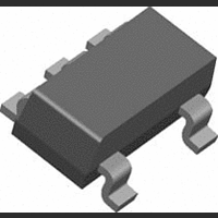
DS90LV012ATMF/NOPB National Semiconductor, DS90LV012ATMF/NOPB Datasheet - Page 3

DS90LV012ATMF/NOPB
Manufacturer Part Number
DS90LV012ATMF/NOPB
Description
IC LINE RCVR SGL 3V LVDS SOT23-5
Manufacturer
National Semiconductor
Type
Receiverr
Datasheet
1.DS90LT012ATMFNOPB.pdf
(8 pages)
Specifications of DS90LV012ATMF/NOPB
Package / Case
SOT-23-5, SC-74A, SOT-25
Mounting Type
Surface Mount
Voltage - Supply
2.7 V ~ 3.6 V
Number Of Drivers/receivers
0/1
Protocol
LVDS
Supply Current
9mA
Supply Voltage Range
2.7V To 3.6V
Driver Case Style
SOT-23
No. Of Pins
5
Operating Temperature Range
-40°C To +85°C
Msl
MSL 1 - Unlimited
Data Rate Max
400Mbps
Rohs Compliant
Yes
Lead Free Status / RoHS Status
Lead free / RoHS Compliant
Other names
DS90LV012ATMF
Available stocks
Company
Part Number
Manufacturer
Quantity
Price
Company:
Part Number:
DS90LV012ATMF/NOPB
Manufacturer:
ST
Quantity:
1 001
Part Number:
DS90LV012ATMF/NOPB
Manufacturer:
NS/国半
Quantity:
20 000
t
t
t
t
t
t
t
f
Symbol
PHLD
PLHD
SKD1
SKD3
SKD4
TLH
THL
MAX
Switching Characteristics
Over Supply Voltage and Operating Temperature ranges, unless otherwise specified. (Notes 6, 7)
Note 1: “Absolute Maximum Ratings” are those values beyond which the safety of the device cannot be guaranteed. They are not meant to imply that the devices
should be operated at these limits. The table of “Electrical Characteristics” specifies conditions of device operation.
Note 2: Current into device pins is defined as positive. Current out of device pins is defined as negative. All voltages are referenced to ground unless otherwise
specified (such as V
Note 3: All typicals are given for: V
Note 4: ESD Ratings:
DS90LV012A:
DS90LT012A:
Note 5: Output short circuit current (I
exceed maximum junction temperature specification.
Note 6: C
Note 7: Generator waveform for all tests unless otherwise specified: f = 1 MHz, Z
Note 8: t
Note 9: t
V
Note 10: t
recommended operating temperature and voltage ranges, and across process distribution. t
Note 11: V
V
V
Note 12: f
cycle, V
the device over the PVT range by the transition times (t
Parameter Measurement Information
DD
DD
DD
and within 5°C of each other within the operating temperature range.
− 0.3V when V
− 0.3V when V
OL
SKD1
HBM (1.5 kΩ, 100 pF)
EIAJ (0Ω, 200 pF)
CDM
IEC direct (330Ω, 150 pF)
HBM (1.5 kΩ, 100 pF)
EIAJ (0Ω, 200 pF)
CDM
IEC direct (330Ω, 150 pF)
SKD3
Differential Propagation Delay High to Low
Differential Propagation Delay Low to High
Differential Pulse Skew |t
Differential Part to Part Skew (Note 9)
Differential Part to Part Skew (Note 10)
Rise Time
Fall Time
Maximum Operating Frequency (Note 12)
L
(max 0.4V), V
SKD4
MAX
includes probe and jig capacitance.
DD
, part to part skew, is the differential channel-to-channel skew of any event between devices. This specification applies to devices at the same
is the magnitude difference in differential propagation delay time between the positive-going-edge and the negative-going-edge of the same channel.
≥
≥
is always higher than IN+ and IN− voltage. IN+ and IN− are allowed to have voltage range −0.05V to +2.35V when V
generator input conditions: t
, part to part skew, is the differential channel-to-channel skew of any event between devices. This specification applies to devices over the
2000V
2000V
DD
DD
ID
).
= 3.0V to 3.6V. V
= 3.0V to 3.6V.
OH
(min 2.4V), load = 15 pF (stray plus probes). The parameter is guaranteed by design. The limit is based on the statistical analysis of
≥
≥
900V
700V
≥
≥
FIGURE 1. Receiver Propagation Delay and Transition Time Test Circuit
2kV
2kV
DD
≥
≥
OS
= +3.3V and T
5kV
7kV
) is specified as magnitude only, minus sign indicates direction only. Only one output should be shorted at a time, do not
ID
PHLD
Parameter
is not allowed to be greater than 100 mV when V
r
= t
− t
f
< 1 ns (0% to 100%), 50% duty cycle, differential (1.05V to 1.35 peak to peak). Output criteria: 60%/40% duty
PLHD
A
= +25°C.
| (Note 8)
TLH
and t
THL
).
3
O
= 50Ω, t
C
V
(Figure 1 and Figure 2)
ID
L
CM
= 15 pF
r
SKD4
= 200 mV
and t
= 0.05V to 2.35V when V
Conditions
is defined as |Max − Min| differential propagation delay.
f
(0% to 100%)
20015003
≤
3 ns for IN±.
DD
= 2.7V or when V
Min
200
1.0
1.0
0
0
0
DD
Typ
100
350
175
250
= 2.7V and |V
1.8
1.7
0.3
0.4
CM
= |V
Max
www.national.com
400
800
800
3.5
3.5
1.0
1.5
ID
ID
| / 2 to
| / 2 to
Units
MHz
ns
ns
ps
ns
ns
ps
ps


