DS90C031TMX/NOPB National Semiconductor, DS90C031TMX/NOPB Datasheet - Page 7
DS90C031TMX/NOPB
Manufacturer Part Number
DS90C031TMX/NOPB
Description
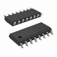
IC LINE DRVR LVDS QUAD 16-SOIC
Manufacturer
National Semiconductor
Type
Driverr
Datasheet
1.DS90C031TMNOPB.pdf
(14 pages)
Specifications of DS90C031TMX/NOPB
Number Of Drivers/receivers
4/0
Protocol
LVDS
Voltage - Supply
4.5 V ~ 5.5 V
Mounting Type
Surface Mount
Package / Case
16-SOIC (3.9mm Width)
Lead Free Status / RoHS Status
Lead free / RoHS Compliant
Other names
*DS90C031TMX
*DS90C031TMX/NOPB
DS90C031TMX
DS90C031TMXTR
*DS90C031TMX/NOPB
DS90C031TMX
DS90C031TMXTR
Available stocks
Company
Part Number
Manufacturer
Quantity
Price
Company:

Part Number:
DS90C031TMX/NOPB
Manufacturer:
TAIYO
Quantity:
440 000


Note 1: “Absolute Maximum Ratings” are those values beyond which the safety of the device cannot be guaranteed. They are not meant to imply that the devices
should be operated at these limits. The table of “Electrical Characteristics” specifies conditions of device operation.
Note 2: Current into device pins is defined as positive. Current out of device pins is defined as negative. All voltages are referenced to ground except: V
Note 3: All typicals are given for: V
Note 4: Channel-to-Channel Skew is defined as the difference between the propagation delay of the channel and the other channels in the same chip with an event
on the inputs.
Note 5: Chip to Chip Skew is defined as the difference between the minimum and maximum specified differential propagation delays.
Note 6: Generator waveform for all tests unless otherwise specified: f = 1 MHz, Z
Note 7: ESD Ratings:
Note 8: Output short circuit current (I
Note 9: C
Note 10: Guaranteed by characterization data (DS90C031E).
Applications Information
The footprint of the DS90C031 is the same as the industry
standard 26LS31 Quad Differential (RS-422) Driver.
Pin Descriptions
V
OD1
Pin No.
(SOIC)
10, 14
11, 13
HBM (1.5 k , 100 pF)
EIAJ (0 , 200 pF)
9, 15
1, 7,
2, 6,
3, 5,
12
.
4
L
includes probe and jig capacitance.
D
D
Name
EN*
D
OUT+
OUT−
EN
IN
250V
3,500V
Driver input pin, TTL/CMOS
compatible
Non-inverting driver output pin,
LVDS levels
Inverting driver output pin,
LVDS levels
Active high enable pin, OR-ed
with EN*
Active low enable pin, OR-ed
with EN
CC
OS
= +5.0V, T
) is specified as magnitude only, minus sign indicates direction only.
Description
A
= +25˚C.
(Continued)
FIGURE 7. Driver Output Levels
7
O
= 50 , t
Ordering Information
DS90C031E-QML
5962-95833
−55˚C to +125˚C
Pin No.
−40˚C to +85˚C
(SOIC)
Temperature
16
Operating
8
r
6 ns, and t
Name
GND
V
f
CC
6 ns.
Package Type/
(NSID)
(SMD)
Power supply pin, +5V
Ground pin
SOP/M16A
LCC/E20A
Number
Description
DS011946-9
DS90C031E-QML
Order Number
DS90C031TM
www.national.com
±
10%
OD1
and
Related parts for DS90C031TMX/NOPB
Image
Part Number
Description
Manufacturer
Datasheet
Request
R

Part Number:
Description:
IC LINE DRVR LVDS QUAD 16-SOIC
Manufacturer:
National Semiconductor
Datasheet:

Part Number:
Description:
IC, DIFFERENTIAL LINE DRIVER, SOIC-16
Manufacturer:
National Semiconductor
Datasheet:

Part Number:
Description:
Manufacturer:
National Semiconductor
Datasheet:
Part Number:
Description:
National Semiconductor [8-Bit D/A Converter]
Manufacturer:
National Semiconductor
Datasheet:
Part Number:
Description:
National Semiconductor [Media Coprocessor]
Manufacturer:
National Semiconductor
Datasheet:
Part Number:
Description:
Digitally Controlled Tone and Volume Circuit with Stereo Audio Power Amplifier, Microphone Preamp Stage and National 3D Sound
Manufacturer:
National Semiconductor
Datasheet:
Part Number:
Description:
Digitally Controlled Tone and Volume Circuit with Stereo Audio Power Amplifier, Microphone Preamp Stage and National 3D Sound
Manufacturer:
National Semiconductor
Datasheet:
Part Number:
Description:
AC97 Rev 2 Codec with Sample Rate Conversion and National 3D Sound
Manufacturer:
National Semiconductor
Part Number:
Description:
Manufacturer:
National Semiconductor
Datasheet:
Part Number:
Description:
Manufacturer:
National Semiconductor
Datasheet:
Part Number:
Description:
General Purpose, Low Voltage, Low Power, Rail-to-Rail Output Operational Amplifiers
Manufacturer:
National Semiconductor
Datasheet:
Part Number:
Description:
8-bit 20 MSPS flash A/D converter.
Manufacturer:
National Semiconductor
Datasheet:
Part Number:
Description:
Low Noise Quad Operational Amplifier
Manufacturer:
National Semiconductor
Datasheet:
Part Number:
Description:
Quad Differential Line Receivers
Manufacturer:
National Semiconductor
Datasheet: