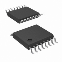
DS90LV032ATMTCX/NOPB National Semiconductor, DS90LV032ATMTCX/NOPB Datasheet - Page 2

DS90LV032ATMTCX/NOPB
Manufacturer Part Number
DS90LV032ATMTCX/NOPB
Description
IC LINE RVR 3V QUAD DIFF 16TSSOP
Manufacturer
National Semiconductor
Type
Receiverr
Datasheet
1.DS90LV032ATMTCNOPB.pdf
(12 pages)
Specifications of DS90LV032ATMTCX/NOPB
Number Of Drivers/receivers
0/4
Protocol
RS644
Voltage - Supply
3 V ~ 3.6 V
Mounting Type
Surface Mount
Package / Case
16-TSSOP
Lead Free Status / RoHS Status
Lead free / RoHS Compliant
Other names
*DS90LV032ATMTCX
*DS90LV032ATMTCX/NOPB
DS90LV032ATMTCX
*DS90LV032ATMTCX/NOPB
DS90LV032ATMTCX
Available stocks
Company
Part Number
Manufacturer
Quantity
Price
Company:
Part Number:
DS90LV032ATMTCX/NOPB
Manufacturer:
NS/TI
Quantity:
20
Part Number:
DS90LV032ATMTCX/NOPB
Manufacturer:
NS/国半
Quantity:
20 000
www.national.com
Symbol
V
V
VCMR
I
V
V
I
I
V
V
I
V
I
I
IN
OS
OZ
I
CC
CCZ
TH
TL
OH
OL
IH
IL
CL
Absolute Maximum Ratings
If Military/Aerospace specified devices are required,
please contact the National Semiconductor Sales Office/
Distributors for availability and specifications.
Electrical Characteristics
Over Supply Voltage and Operating Temperature ranges, unless otherwise specified.
Supply Voltage (V
Input Voltage (R
Enable Input Voltage (EN, EN*)
Output Voltage (R
Maximum Package Power Dissipation @ +25°C
Storage Temperature Range
M Package
MTC Package
Derate M Package
Derate MTC Package
Differential Input High Threshold
Differential Input Low Threshold
Common-Mode Voltage Range
Input Current
Output High Voltage
Output Low Voltage
Output Short Circuit Current
Output TRI-STATE Current
Input High Voltage
Input Low Voltage
Input Current
Input Clamp Voltage
No Load Supply Current
Receivers Enabled
No Load Supply Current
Receivers Disabled
IN+
Parameter
CC
OUT
, R
)
)
IN−
)
8.2 mW/°C above +25°C
6.9 mW/°C above +25°C
−0.3V to (V
−0.3V to (V
−65°C to +150°C
V
(Note
VID = 200 mV peak to peak
V
V
V
I
I
I
I
Enabled, V
Disabled, V
V
I
EN, EN* = V
EN, EN* = 2.4V or 0.5V, Inputs Open
EN = GND, EN* = V
OH
OH
OH
OL
CL
−0.3V to +3.9V
CM
IN
IN
IN
IN
= −18 mA
−0.3V to +4V
= 2 mA, V
= +2.8V
= 0V
= +3.6V
= −0.4 mA, V
= −0.4 mA, Input terminated
= −0.4 mA, Input shorted
= 0V or V
= +1.2V
(Note
CC
CC
13)
1025 mW
866 mW
+ 0.3V)
+ 0.3V)
1)
OUT
OUT
CC
CC
ID
= 0V
or GND, Inputs Open
= 0V or V
, Other Input = V
= −200 mV
V
V
Conditions
ID
CC
CC
= +200 mV
CC
(Note
= 3.6V or 0V
= 0V
2
, Inputs Open
CC
Supply Voltage (V
Receiver Input Voltage
Operating Free Air
Lead Temperature Range
Maximum Junction Temperature
ESD Rating
11)
Temperature (T
(Soldering 4 sec.)
(HBM 1.5 kΩ, 100 pF)
(EIAJ 0 Ω, 200 pF)
(Note
CC
5)
or GND
(Note
Recommended Operating
(Note
A
CC
10)
)
)
R
R
R
EN*
EN,
V
Pin
OUT
IN+
2)
IN−
CC
Conditions
,
GND
+3.0
Min
−40
−100
GND
−1.5
Min
−10
−10
−15
−10
−10
-20
0.1
2.7
2.7
2.7
2.0
+3.3
Typ
25
−0.8
Typ
+20
−20
−48
3.0
3.0
3.0
0.1
±1
±1
±1
±1
10
10
3
+3.6
+3.0
Max
+85
+100
−120
Max
0.25
+10
+10
+20
+10
V
+10
2.3
0.8
15
15
5
CC
≥
≥
+260°C
+150°C
Units
4.5 kV
250 V
°C
V
V
Units
mV
mV
mA
mA
mA
mA
μA
μA
μA
μA
μA
V
V
V
V
V
V
V
V


