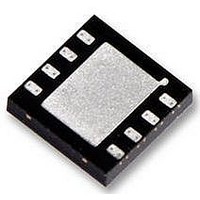
LMH6553SD National Semiconductor, LMH6553SD Datasheet - Page 19

LMH6553SD
Manufacturer Part Number
LMH6553SD
Description
DIFF AMP, 900MHZ, 8LLP, POWERWISE
Manufacturer
National Semiconductor
Datasheet
1.LMH6553SDE.pdf
(24 pages)
Specifications of LMH6553SD
No. Of Amplifiers
1
Gain Db Max
1dB
Bandwidth
900MHz
Slew Rate
2300V/µs
Supply Voltage Range
4.5V To 12V
Supply Current
29.1mA
Amplifier Case Style
LLP
No. Of Pins
8
Rohs Compliant
Yes
OUTPUT NOISE PERFORMANCE AND MEASUREMENT
Unlike differential amplifiers based on voltage feedback ar-
chitectures, noise sources internal to the LMH6553 refer to
the inputs largely as current sources, hence the low input re-
ferred voltage noise and relatively higher input referred cur-
rent noise. The output noise is therefore more strongly
coupled to the value of the feedback resistor and not to the
closed loop gain, as would be the case with a voltage feed-
back differential amplifier. This allows operation of the
LMH6553 at much higher gain without incurring a substantial
noise performance penalty, simply by choosing a suitable
feedback resistor.
Figure 9 shows a circuit configuration used to measure noise
figure for the LMH6553 in a 50Ω system. An R
275Ω is chosen for the PSOP package to minimize output
noise while simultaneously allowing both high gain (9 V/V)
and proper 50Ω input termination. Refer to the section titled
Single-Ended Input Operation for calculation of resistor and
gain values. Noise figure values at various frequencies are
shown in the plot titled Noise Figure in the Typical Perfor-
mance Characteristics section.
DRIVING ANALOG TO DIGITAL CONVERTERS
Analog-to-digital converters present challenging load condi-
tions. They typically have high impedance inputs with large
and often variable capacitive components. As well, there are
usually current spikes associated with switched capacitor or
sample and hold circuits. Figure 10 shows the LMH6553 driv-
ing the ADC14C105. The amplifier is configured to provide a
gain of 2 V/V in a single-to-differential mode. The LMH6553
common mode voltage is set by the ADC14C105. The 0.1 µF
capacitor, in series with the 49.9Ω resistor, is inserted to
ground across the 68.1Ω resistor to balance the amplifier in-
puts. The circuit in Figure 10 has a 2nd order lowpass LC filter
formed by the 620 nH inductors along with the 22 pF capacitor
across the differential inputs of the ADC14C105. The filter has
a pole frequency of about 50 MHz. The two 100Ω resistors
serve to isolate the capacitive loading of the ADC from the
amplifier and ensure stability. For switched capacitor input
ADCs, the input capacitance will vary based on the clock cy-
cle, as the ADC switches between the sample and hold mode.
See your particular ADC's datasheet for details.
FIGURE 9. Noise Figure Circuit Configuration
F
value of
30043750
19
Figure 11 shows the SFDR and SNR performance vs. fre-
quency for the LMH6553 and ADC14C105 combination cir-
cuit with the ADC input signal level at −1 dBFS. The
ADC14C105 is a single channel 14-bit ADC with maximum
sampling rate of 105 MSPS. The amplifier is configured to
provide a gain of 2 V/V in single to differential mode. An ex-
ternal bandpass filter is inserted in series between the input
signal source and the amplifier to reduce harmonics and noise
from the signal generator. In order to properly match the input
impedance seen at the LMH6553 amplifier inputs, R
sen to match Z
The amplifier and ADC should be located as close together
as possible. Both devices require that the filter components
be in close proximity to them. The amplifier needs to have
minimal parasitic loading on it's outputs and the ADC is sen-
sitive to high frequency noise that may couple in on its inputs.
Some high performance ADCs have an input stage that has
a bandwidth of several times its sample rate. The sampling
process results in all input signals presented to the input stage
mixing down into the first Nyquist zone (DC to Fs/2).
The LMH6553 is capable of driving a variety of National Semi-
conductor Analog-to-Digital Converters. This is shown in Ta-
ble 3, which offers a list of possible signal path ADC and
amplifier combinations. The use of the LMH6553 to drive an
ADC is determined by the application and the desired sam-
pling process (Nyquist operation, sub-sampling or over-sam-
pling). See application note AN-236 for more details on the
sampling processes and application note AN-1393 'Using
FIGURE 11. LMH6553/ADC14C105 SFDR and SNR
FIGURE 10. Driving a 14-bit ADC
S
Performance vs. Frequency
|| R
T
for proper input balance.
www.national.com
30043768
M
is cho-
30043766


