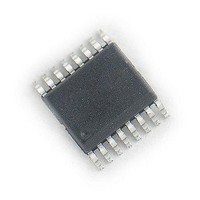
NJM2626V-TE1 NJR, NJM2626V-TE1 Datasheet

NJM2626V-TE1
Specifications of NJM2626V-TE1
Related parts for NJM2626V-TE1
NJM2626V-TE1 Summary of contents
Page 1
... Forward or Reverse direction Internal Soft Start -External capacitor to Verr pin Internal ON/OFF Circuit -No-output is Verr pin to GND Bipolar Technology Package Outline Ver.2009-02-26 ! Package Outline NJM2626V Vcc 26V Current limit=0.5V±10% Internal pull-up resistor 10k SSOP-16/ SSOP20-C3 NJM2626 NJM2626VC3 - 1 - ...
Page 2
NJM2626 ! ABSOLUTE MAXIMUM RATINGS PARAMETER Logic Supply Voltage Maximum Output Current Power Dissipation (SSOP-16) Power Dissipation (SSOP20-C3) Operating Temperature Range Storage Temperature range (*1): Mounted on the glass epoxy board based on EIA/JEDEC. (114.3x76.2x1.6mm: 2Layer/4Layer SYNBO ...
Page 3
ELECTRICAL CHARACTERISTICS PARAMETER ! General Operation Supply Voltage Under Voltage Sense Voltage Hysteresis Voltage (Under Voltage Lock Out) Supply Current ! Reference Voltage Section Reference Voltage Output Line Regulation Load Regulation ! Hall Amplifier Section Input H Level Voltage ...
Page 4
NJM2626 ! ELECTRICAL CHARACTERISTICS PARAMETER SYMBOL ! Error Amplifier Section Input Offset Voltage Input Bias Current Input Common Mode Voltage Range ! Forward/ Reverse Direction Section (FR input terminal) Output Forward Direction Output Reverse Direction Hysteresis Voltage Ratio Pull-Up Resistance ...
Page 5
PIN CONFIGURATION FR 1 Vref OSC 6 Verr 7 GND 8 SSOP-16 Ver.2009-02-26 VCC Vref OSC VL 11 ...
Page 6
NJM2626 ! BLOCK DIAGRAM VCC H1 VCC H2 VCC H3 VCC Vref Vref Saw OSC Osillator Verr + - GND - Vref Rotor Position Decode VCC UVLO Logic + - + - ...
Page 7
TYPICAL CHARACTERISTICS ICC vs. VCC 25 Ta=25degC H1=H2=H3=0V output=Open OSC=1000pF 20 Verr= VCC [V] UVLO vs. Temperature 6 output=Open OSC=1000pF Verr=3.5V 5.5 5 4 Temperature [degC] ...
Page 8
TYPICAL CHARACTERISTICS Vref vs. Temperature VCC=12V H1=H2=H3=0V 4.4 output=Open OSC=1000pF Verr=0V 4.2 4 3.8 3.6 - Temperature [degC] VhH-L vs. Temperature 2.5 VCC=12V output=Open OSC=1000pF Verr=3.5V 2 1 Temperature [degC] VOH-d vs. Temperature 12 ...
Page 9
TYPICAL CHARACTERISTICS VCL vs. Temperature 18 VCC=28V output=Open OSC=1000pF Verr=3.5V 17.5 17 16.5 16 15 Temperature [degC] fosc vs. VCC 35 Ta=25degC H1=H2=H3=0V output=Open OSC=1000pF Verr= VCC ...


