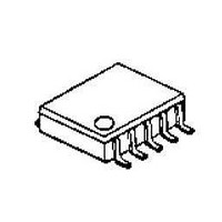
NJU7329ARB2-TE1 NJR, NJU7329ARB2-TE1 Datasheet - Page 8

NJU7329ARB2-TE1
Manufacturer Part Number
NJU7329ARB2-TE1
Description
Motor / Motion / Ignition Controllers & Drivers Single Phase DC Brushless Mtr Drvr
Manufacturer
NJR
Type
Single Phase DC Brushless Motor Driver ICr
Datasheet
1.NJU7329ARB2-TE1.pdf
(9 pages)
Specifications of NJU7329ARB2-TE1
Operating Supply Voltage
7 V
Supply Current
4 mA
Mounting Style
SMD/SMT
Package / Case
TVSP-10
Operating Temperature
85 C
Lead Free Status / Rohs Status
Lead free / RoHS Compliant
NJU7329B
3. Design of hall element bias resistance (R1 and R2)
4. Design of FG output resistsnce (R3)
- 8 -
A typical value of C2 is either 0.47uF or 1uF depending on a motor.
Ct Terminal voltage
range.Non-excitation hall bias voltage is to be set at a half of V
range. Therefore the same value of hall bias resistors is selected for R1 and R2.
be obtained.
of FG Out is as follows.
The common-mode input voltage is between 0.4V and V
Given that the bias current is set to be 5mA by HW101A datasheet, R1 and R2 can be determined as follows:
The output voltage of hall elements is influenced by the bias current and magnetic flux density of hall elements.
The optimum input voltage of NJU7329B is 100mVp-p and higher. With such input voltage, the highest efficiency can
FG Out(FG:Pin8) is a open drain output and R3 is a pull up register. A typical value of R3 is 10k . The timing chart
Hall amplifier is a differential amplifier with hysteresis characteristics (24mV typical).
Motor output
R
R
FG Terminal voltage
1
1
Hall input
R
R
2
2
Rin
300
Hall input
Ihbias
V
IN+
DD
5
10
5
3
Motor Locked
1
k
Motor Lock protection period
Toff
DD
DD
-1V and the input signal must be within the
for effective use of common-mode input voltage
Ton
Returns to normal operation


