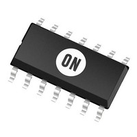
UC3844DR2 ON Semiconductor, UC3844DR2 Datasheet - Page 6

UC3844DR2
Manufacturer Part Number
UC3844DR2
Description
Other Power Management 52kHz 1A Current PWM
Manufacturer
ON Semiconductor
Type
High Performance Current Mode Controllersr
Datasheet
1.UC2845DR2.pdf
(16 pages)
Specifications of UC3844DR2
Output Voltage Range
4.9 V to 5.1 V
Input Voltage Range
30 V
Operating Temperature Range
0 C to + 70 C
Mounting Style
SMD/SMT
Package / Case
SOIC-14
Lead Free Status / Rohs Status
Lead free / RoHS Compliant
PIN FUNCTION DESCRIPTION
8−Pin
1
2
3
4
5
6
7
8
−
−
−
−
Pin
2,4,6,13
14−Pin
Figure 14. Output Cross Conduction
10
12
14
11
1
3
5
7
−
8
9
Compensation
Current Sense
Power Ground
Feedback
Function
Voltage
Output
R
GND
GND
100 ns/DIV
V
V
NC
T
V
CC
ref
/C
C
T
This pin is Error Amplifier output and is made available for loop compensation.
This is the inverting input of the Error Amplifier. It is normally connected to the switching
power supply output through a resistor divider.
A voltage proportional to inductor current is connected to this input. The PWM uses this
information to terminate the output switch conduction.
The Oscillator frequency and maximum Output duty cycle are programmed by connecting
resistor R
This pin is combined control circuitry and power ground (8−pin package only).
This output directly drives the gate of a power MOSFET. Peak currents up to 1.0 A are
sourced and sunk by this pin. The output switches at one−half the oscillator frequency.
This pin is the positive supply of the control IC.
This is the reference output. It provides charging current for capacitor C
This pin is a separate power ground return (14−pin package only) that is connected back to
the power source. It is used to reduce the effects of switching transient noise on the control
circuitry.
The Output high state (V
With a separate power source connection, it can reduce the effects of switching transient
noise on the control circuitry.
This pin is the control circuitry ground return (14−pin package only) and is connected to back
to the power source ground.
No connection (14−pin package only). These pins are not internally connected.
V
C
T
A
CC
L
T
= 255C
= 15 pF
to V
= 30 V
http://onsemi.com
ref
and capacitor C
6
OH
) is set by the voltage applied to this pin (14−pin package only).
25
20
15
10
5
0
0
T
to ground. Operation to 1.0 MHz is possible.
Description
Figure 15. Supply Current versus
10
V
CC
Supply Voltage
, SUPPLY VOLTAGE (V)
20
T
through resistor R
R
C
V
I
T
Sense
30
A
FB
T
T
= 255C
= 10 k
= 3.3 nF
= 0 V
= 0 V
40
T
.


