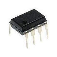
CAT1161PI-42 Catalyst / ON Semiconductor, CAT1161PI-42 Datasheet

CAT1161PI-42
Specifications of CAT1161PI-42
Related parts for CAT1161PI-42
CAT1161PI-42 Summary of contents
Page 1
... Supervisory Circuits with I Precision Reset Controller and Watchdog Timer (16K) FEATURES Watchdog monitors SDA signal (CAT1161) 2 400kHz I C bus compatible 2.7V to 6.0V operation Low power CMOS technology 16-Byte page write buffer Built-in inadvertent write protection — V lock out CC — Write protect pin, WP Active high or low reset — ...
Page 2
CAT1161, CAT1162 BLOCK DIAGRAM EXTERNA L LOAD D OUT ACK V CC WORDADDRESS GND BUFFERS START/STOP SDA LOGIC XDEC CONTR OL WP LOGIC RESET Controller Precision WATCHDOG Only for Vcc Monitor CAT1161 RESET RESET ABSOLUTE MAXIMUM RATINGS Parameters Temperature Under ...
Page 3
D.C. OPERATING CHARACTERISTICS V = 2.7V to 6V, unless otherwise specified. CC Symbol Parameter I Power Supply Current CC I Standby Current SB I Input Leakage Current LI I Output Leakage Current LO V Input Low Voltage IL V Input ...
Page 4
CAT1161, CAT1162 WRITE CYCLE LIMITS Symbol Parameter t Write Cycle Time WR The write cycle time is the time from a valid stop condition of a write sequence to the end of the internal program/erase cycle. During the write cycle, ...
Page 5
PIN DESCRIPTION WP: WRITE PROTECT If the pin is tied to V the entire memory array CC becomes Write Protected (READ only). When the pin is tied to GND or left floating normal read/write operations are allowed to the device. ...
Page 6
CAT1161, CAT1162 Hardware Data Protection The CAT1161/2 is designed with the following hardware data protection features to provide a high degree of data integrity. (1) The CAT1161/2 features a WP pin. When the WP pin is tied high the entire ...
Page 7
FUNCTIONAL DESCRIPTION 2 The CAT1161/2 supports the I C Bus data transmis– sion protocol. This Inter-Integrated Circuit Bus proto– col defines any device that sends data to the bus transmitter and any device receiving data to be ...
Page 8
CAT1161, CAT1162 Acknowledge After a successful data transfer, each receiving device is required to generate an acknowledge. The acknowledging device pulls down the SDA line during the ninth clock cycle, signaling that it received the 8 bits of data. The ...
Page 9
Acknowledge Polling Disabling of the inputs can be used to take advantage of the typical write cycle time. Once the stop condition is issued to indicate the end of the host’s write opration, the CAT1161/2 initiates the internal write cycle. ...
Page 10
CAT1161, CAT1162 Selective/Random Read Selective/Random READ operations allow the Master device to select at random any memory location for a READ operation. The Master device first performs a ‘dummy’ write operation by sending the START condition, slave address and byte ...
Page 11
PACKAGE OUTLINE DRAWINGS (1)(2) PDIP 8-Lead 300mils (L) PIN # 1 IDENTIFICATION D TOP VIEW SIDE VIEW Notes: (1) All dimensions are in millimeters. (2) Complies with JEDEC MS-001. © 2009 SCILLC. All rights reserved. Characteristics subject ...
Page 12
CAT1161, CAT1162 (1)(2) SOIC 8-Lead 150mils (W) PIN # 1 IDENTIFICATION TOP VIEW SIDE VIEW Notes: (1) All dimensions are in millimeters. Angles in degrees. (2) Complies with JEDEC MS-012. Doc. No. MD-3002 Rev. I SYMBOL A ...
Page 13
EXAMPLE OF ORDERING INFORMATION Prefix Device # Suffix CAT 1162 W Optional Company ID Product Package L: Number 1161: 16K W: SOIC 1162: 16K ORDERING INFORMATION Orderable Part Number Reset Threshold Voltage CAT1161LI-25-G CAT1161LI-28-G CAT1161LI-30-G CAT1161LI-42-G CAT1161LI-45-G CAT1161WI-25-GT3 CAT1161WI-28-GT3 CAT1161WI-30-GT3 ...
Page 14
CAT1161, CAT1162 REVISION HISTORY Date Rev. Description Add Green Logo 17-Feb-05 E Add Package Outline Update Ordering Information Update Package Outline 2-Feb-07 F Update Example of Ordering Information Update Package Outline Drawings 28-Nov07 G Update Example of Ordering Information Add ...


