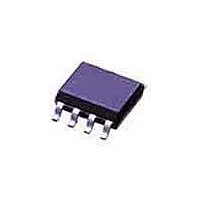
CAT1162JI-42 Catalyst / ON Semiconductor, CAT1162JI-42 Datasheet - Page 8

CAT1162JI-42
Manufacturer Part Number
CAT1162JI-42
Description
Supervisory Circuits 16K I2C Mem w/Reset
Manufacturer
Catalyst / ON Semiconductor
Datasheet
1.CAT1161WI-45-T3.pdf
(14 pages)
Specifications of CAT1162JI-42
Number Of Voltages Monitored
1
Monitored Voltage
3 V, 3.3 V, 5 V
Output Type
Active High, Active Low, Open Drain
Manual Reset
Resettable
Watchdog
No Watchdog
Battery Backup Switching
No Backup
Supply Voltage (max)
6 V
Supply Voltage (min)
2.7 V
Supply Current (typ)
3000 uA
Maximum Power Dissipation
1000 mW
Maximum Operating Temperature
+ 85 C
Mounting Style
SMD/SMT
Package / Case
SOIC-8
Minimum Operating Temperature
- 40 C
Power Fail Detection
No
Undervoltage Threshold
4.25 V
Overvoltage Threshold
4.5 V
Lead Free Status / Rohs Status
Lead free / RoHS Compliant
CAT1161, CAT1162
Acknowledge
After a successful data transfer, each receiving
device is required to generate an acknowledge. The
acknowledging device pulls down the SDA line
during the ninth clock cycle, signaling that it received
the 8 bits of data.
The CAT1161/2 responds with an acknowledge after
receiving a START condition and its slave address.
If the device has been selected along with a write
operation, it responds with an acknowledge after
receiving each 8-bit byte.
When the CAT1161/2 begins a READ mode it
transmits 8 bits of data, releases the SDA line and
monitors the line for an acknowledge. Once it
receives this acknowledge, the CAT1161/2 will
continue to transmit data. If no acknowledge is sent
by
transmission and waits for a STOP condition.
WRITE OPERATIONS
Byte Write
In the Byte Write mode, the Master device sends the
START condition and the slave address information
(with the R/W ¯ ¯ bit set to zero) to the Slave device.
After the Slave generates an acknowledge, the
Master sends a 8-bit address that is to be written
into the address pointers of the CAT1161/2. After
Figure 7. Byte Write Timing
Figure 8. Page Write Timing
Doc. No. MD-3002 Rev. I
the
BUS ACTIVITY:
Master,
SDA LINE
MASTER
the
S
BUS ACTIVITY:
S
T
A
R
T
device
SDA LINE
ADDRESS
MASTER
SLAVE
terminates
S
S
T
A
R
T
A
C
K
ADDRESS (n)
ADDRESS
SLAVE
BYTE
data
A
C
K
A
C
K
8
receiving another acknowledge from the Slave, the
Master device transmits the data to be written into the
addressed memory location. The CAT1161/2 acknow–
ledges once more and the Master generates the STOP
condition. At this time, the device begins an internal
programming cycle to non-volatile memory. While the
cycle is in progress, the device will not respond to any
request from the Master device.
Page Write
The CAT1161/2 writes up to 16 bytes of data in a single
write cycle, using the Page Write operation. The page
write operation is initiated in the same manner as the
byte write operation, however instead of terminating
after the initial byte is transmitted, the Master is allowed
to send up to 15 additional bytes. After each byte has
been transmitted, the CAT1161/2 will respond with an
acknowledge and internally increment the lower order
address bits by one. The high order bits remain
unchanged.
If the Master transmits more than 16 bytes before
sending the STOP condition, the address counter
‘wraps around,’ and previously transmitted data will be
overwritten.
When all 16 bytes are received, and the STOP
condition has been sent by the Master, the internal
programming cycle begins. At this point, all received
data is written to the CAT1161/2 in a single write cycle.
ADDRESS
BYTE
DATA n
A
C
K
C
A
K
DATA n+1
DATA
A
C
K
Characteristics subject to change without notice
C
A
K
P
O
S
T
P
© 2009 SCILLC. All rights reserved.
DATA n+15
C
A
K
O
S
T
P
P


