NCP345SNT1G ON Semiconductor, NCP345SNT1G Datasheet
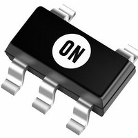
Supervisory Circuits 6.85V OVP Supervisor

NCP345SNT1G

Manufacturer Part Number
NCP345SNT1G
Description
Supervisory Circuits 6.85V OVP Supervisor
Manufacturer
ON Semiconductor
Datasheet

Specifications of NCP345SNT1G

Number Of Voltages Monitored
1
Monitored Voltage
6.85 V
Overvoltage Threshold
6.85 V
Output Type
PFET Driver
Manual Reset
Resettable
Watchdog
No Watchdog
Supply Voltage (max)
25 V
Supply Voltage (min)
3 V
Supply Current (typ)
750 uA
Maximum Power Dissipation
216 mW
Maximum Operating Temperature
+ 85 C
Mounting Style
SMD/SMT
Package / Case
SOT-23-5 Thin (TSOP-5)
Minimum Operating Temperature
- 40 C
Lead Free Status / Rohs Status
Lead free / RoHS Compliant

Available stocks

Company
Part Number
Manufacturer
Quantity
Price
Part Number:
NCP345SNT1G
Manufacturer:
ONS
Quantity:
11 542
Part Number:
NCP345SNT1G
Manufacturer:
ON/安森美
Quantity:
20 000
Part Number:
NCP345SNT1G
Manufacturer:
ON
Quantity:
19 559
NCP345
Overvoltage Protection IC
sensitive electronic circuitry from overvoltage transients and power
supply faults when used in conjunction with an external P−channel
FET. The device is designed to sense an overvoltage condition and
quickly disconnect the input voltage supply from the load before any
damage can occur. The OVP consists of a precise voltage reference, a
comparator with hysteresis, control logic, and a MOSFET gate driver.
The OVP is designed on a robust BiCMOS process and is intended to
withstand voltage transients up to 30 V.
AC/DC adapter or car accessory charger to power the product and/or
recharge the internal batteries. The nominal overvoltage threshold is
6.85 V so it is suitable for single cell Li−Ion applications as well as 3/4
cell NiCD/NiMH applications.
Features
Typical Applications
© Semiconductor Components Industries, LLC, 2006
March, 2006 − Rev. 6
The NCP345 overvoltage protection circuit (OVP) protects
The device is optimized for applications that have an external
Overvoltage Turn−Off Time of less than 1.0 msec
Accurate Voltage Threshold of 6.85 V (nominal)
Undervoltage Lockout Protection
CNTRL Input Compatible with 1.8 V Logic Levels
Pb−Free Package is Available
Cellular Phones
Digital Cameras
Portable Computers and PDAs
Portable CD and other Consumer Electronics
Accessory Charger
AC/DC Adapter or
IN
GND
Figure 1. Simplified Application Diagram
+
V
ref
Undervoltage
V
CC
Lock Out
Logic
1
CNTRL
Microprocessor port
NCP345
Driver
FET
Note: This device contains 89 active transistors
NCP345SNT1
NCP345SNT1G
†For information on tape and reel specifications,
OUT
including part orientation and tape sizes, please
refer to our Tape and Reel Packaging Specifications
Brochure, BRD8011/D.
P−CH
Device
5
CNTRL
GND
RAD = Specific Device Code
A
Y
W
G
(Note: Microdot may be in either location)
ORDERING INFORMATION
OUT
1
PIN CONNECTIONS &
MARKING DIAGRAM
= Assembly Location
= Year
= Work Week
= Pb−Free Package
http://onsemi.com
1
2
3
Schottky
SOT−23−5
SOT−23−5
(Pb−Free)
Diode
(Top View)
Package
Publication Order Number:
THIN SOT−23−5
+
SN SUFFIX
CASE 483
5
4
C1
V
IN
3000 / Tape &
CC
(7 inch Reel)
Shipping
LOAD
NCP345/D
Reel

Related parts for NCP345SNT1G

NCP345SNT1G Summary of contents

Page 1

... ORDERING INFORMATION Device Package Shipping NCP345SNT1 SOT−23−5 3000 / Tape & NCP345SNT1G SOT−23−5 (7 inch Reel) (Pb−Free) †For information on tape and reel specifications, including part orientation and tape sizes, please refer to our Tape and Reel Packaging Specifications Brochure, BRD8011/D. ...

Page 2

IN ( Pre− regulator R1 R2 Bandgap Reference CNTRL (3) PIN FUNCTION DESCRIPTIONS Pin # Symbol 1 OUT This signal drives the gate of a P−channel MOSFET controlled by the voltage level ...

Page 3

ABSOLUTE MAXIMUM RATINGS (T Rating OUT voltage to GND Input and CNTRL pin voltage to GND V Maximum Range CC Maximum Power Dissipation 85°C A Thermal Resistance Junction to Air Junction Temperature Operating Ambient Temperature V Operating ...

Page 4

Ambient Temperature (°C) Figure 3. Typical V Threshold Variation vs. th Temperature 1.0 0.9 0.8 0.7 0.6 0.5 −40 Figure 5. Typical Supply Current vs. Temperature ...

Page 5

AC/DC Adapter or Accessory Charger IN Zener Diode (optional) GND Introduction In many electronic products, an external AC/DC wall adapter is used to convert the AC line voltage into a regulated DC voltage or a current limited source. Line surges ...

Page 6

Normal Operation Figure 1 illustrates a typical configuration. The external adapter provides power to the protection system so the circuitry is only active when the adapter is connected. The OVP monitors the voltage from the charger and if the voltage ...

Page 7

... H SOLDERING FOOTPRINT* 0.95 0.037 1.0 0.039 *For additional information on our Pb−Free strategy and soldering details, please download the ON Semiconductor Soldering and Mounting Techniques Reference Manual, SOLDERRM/D. NCP345 THIN SOT−23−5 SN SUFFIX CASE 483−02 ISSUE E NOTES: 1. DIMENSIONING AND TOLERANCING PER ANSI Y14 ...

Page 8

... Fax: 480−829−7709 or 800−344−3867 Toll Free USA/Canada Email: orderlit@onsemi.com NCP345 N. American Technical Support: 800−282−9855 Toll Free USA/Canada Japan: ON Semiconductor, Japan Customer Focus Center 2−9−1 Kamimeguro, Meguro−ku, Tokyo, Japan 153−0051 Phone: 81−3−5773−3850 http://onsemi.com 8 ON Semiconductor Website: http://onsemi ...

Related keywords