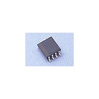
MCP1612-120I/MS Microchip Technology, MCP1612-120I/MS Datasheet - Page 4

MCP1612-120I/MS
Manufacturer Part Number
MCP1612-120I/MS
Description
Switching Converters, Regulators & Controllers 1.4MHz 1A Synch-Buck
Manufacturer
Microchip Technology
Datasheet
1.MCP1612-ADJIMS.pdf
(22 pages)
Specifications of MCP1612-120I/MS
Output Current
1.0 A
Mounting Style
SMD/SMT
Package / Case
MSOP-8
Lead Free Status / Rohs Status
Lead free / RoHS Compliant
MCP1612
1.0
Absolute Maximum Ratings †
V
(SHDN, FB, V
L
P
Output Short Circuit Current ................................. Continuous
Storage temperature .....................................-65°C to +150°C
Ambient Temp. with Power Applied.................-40°C to +85°C
Operating Junction Temperature...................-40°C to +125°C
ESD protection on all pins (HBM)
ESD protection on all pins (MM)
DC CHARACTERISTICS
DS21921A-page 4
Electrical Specifications: Unless otherwise noted, V
I
Input Voltage
Input Operating Voltage
Input Shutdown Current
Input Quiescent Current
Oscillator Characteristics
Internal Oscillator Frequency
Internal Power Swicthes
R
R
L
Positive Current Limit Threshold
Negative Current Limit Threshold
Feedback Characteristics
Transconductance from FB to
COMP
Output Voltage
Output Voltage Range
Reference Feedback Voltage
Feedback Input Bias Current
Line Regulation
Load Regulation
Note 1:
X
IN
GND
LOAD
X
DSon
DSon
to P
Pin Leakage Current
– A
to A
GND
= 100 mA, T
P-Channel
N-Channel
2:
GND
ELECTRICAL
CHARACTERISTICS
GND
.............................................. -0.3V to (V
Parameters
.....................................................................6.0V
The integrated MOSFET switches have an integral diode from the L
these diodes are forward-biased, the package power dissipation limits must be adhered to. Thermal protection is not
able to limit the junction temperature for these cases.
UVLO is specified for a falling V
return to operation.
CC
................................................... -0.3V to +0.3V
, Comp ........... (A
A
= +25°C. Boldface specifications apply over the T
GND
V
V
+I
-I
R
R
LOAD-REG
LINE-REG
– 0.3V) to (V
LX(MAX)
I(V
I(V
F
LX(MAX)
V
Sym
DSon-N
DSon-P
I
V
V
I
g
VFB
OSC
OUT
LX
FB
IN
m
IN
IN
)
)
IN
. Once the UVLO is activated, the UVLO-
IN
IN
0.78
Min
2.7
1.2
0.8
35
—
—
—
—
—
—
—
—
—
+ 0.3V)
+ 0.3V)
-1
IN
300 V
4 kV
= V
cc
= V
0.01
0.15
0.25
Typ
300
300
-1.4
1.4
2.3
0.8
—
—
62
—
5
1
SHDN
A
† Notice: Stresses above those listed under “Maximum
Ratings” may cause permanent damage to the device. This is
a stress rating only and functional operation of the device at
those or any other conditions above those indicated in the
operational listings of this specification is not implied.
Exposure to maximum rating conditions for extended periods
may affect device reliability.
= 3.3V, V
range of -40°C to +85°C.
Max
0.82
V
5.5
1.6
0.5
90
—
—
—
—
—
—
1
7
1
IN
X
OUT
pin to V
= 1.8V, C
Units
µA/V
MHz
%/V
m
m
mA
µA
µA
nA
HYS
%
V
A
A
V
V
IN
must be overcome before the device will
and from L
Shutdown mode (SHDN = GND)
I
I
I
SHDN = 0V, V
L
V
V
IN
LOAD
P
N
X
IN
IN
= 250 mA
= 250 mA
= C
= 5.5V
2004 Microchip Technology Inc.
= 2.7V to 5.5V, I
= 4.2V, I
= 0 mA
OUT
X
to P
= 10 µF, L = 3.3 µH,
LOAD
Conditions
IN
GND
= 5.5V, L
= 100 mA to 1A
. In cases where
LOAD
= 100 mA
X
= 0V,


