DP83848CVV/NOPB National Semiconductor, DP83848CVV/NOPB Datasheet - Page 14
DP83848CVV/NOPB
Manufacturer Part Number
DP83848CVV/NOPB
Description
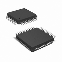
IC TXRX ETHERNET PHYTER 48-LQFP
Manufacturer
National Semiconductor
Type
Transceiverr
Datasheet
1.DP83848CVVXNOPB.pdf
(84 pages)
Specifications of DP83848CVV/NOPB
Number Of Drivers/receivers
1/1
Protocol
Ethernet
Voltage - Supply
3 V ~ 3.6 V
Mounting Type
Surface Mount
Package / Case
48-LQFP
For Use With
DP83848C-POE-EK - BOARD EVALUATION DP83848CDP83848C-MAU-EK - BOARD EVALUATION DP83848C
Lead Free Status / RoHS Status
Lead free / RoHS Compliant
Other names
*DP83848CVV
*DP83848CVV/NOPB
DP83848CVV
DP83848CVVNOPB
DP83848CVVNOPB
DP83848CVVNOPBTR
DP83848CVVNOPBTR
*DP83848CVV/NOPB
DP83848CVV
DP83848CVVNOPB
DP83848CVVNOPB
DP83848CVVNOPBTR
DP83848CVVNOPBTR
Available stocks
Company
Part Number
Manufacturer
Quantity
Price
Company:

Part Number:
DP83848CVV/NOPB
Manufacturer:
TI
Quantity:
7 600
Company:
Part Number:
DP83848CVV/NOPB
Manufacturer:
NS
Quantity:
4 021
Company:
Part Number:
DP83848CVV/NOPB
Manufacturer:
Texas Instruments
Quantity:
10 000
Part Number:
DP83848CVV/NOPB
Manufacturer:
TI/德州仪器
Quantity:
20 000


www.national.com
1.7 10 Mb/s and 100 Mb/s PMD Interface
1.8 Special Connections
1.9 Power Supply Pins
TD-, TD+
RD-, RD+
RBIAS
PFBOUT
PFBIN1
PFBIN2
RESERVED
RESERVED
IOVDD33
IOGND
DGND
AVDD33
AGND
Signal Name
Signal Name
Signal Name
Type
Type
I/O
I/O
I/O
I/O
O
I
I
32, 48
35, 47
15, 19
Pin #
36
22
8, 9, 10, 11,
16, 17
13, 14
20, 21
Pin #
Pin #
24
23
18
37
12
Differential common driver transmit output (PMD Output Pair).
These differential outputs are automatically configured to either
10BASE-T or 100BASE-TX signaling.
In Auto-MDIX mode of operation, this pair can be used as the Re-
ceive Input pair.
These pins require 3.3V bias for operation.
Differential receive input (PMD Input Pair). These differential in-
puts are automatically configured to accept either 100BASE-TX
or 10BASE-T signaling.
In Auto-MDIX mode of operation, this pair can be used as the
Transmit Output pair.
These pins require 3.3V bias for operation.
Bias Resistor Connection. A 4.87 k
nected from RBIAS to GND.
Power Feedback Output. Parallel caps, 10 F (Tantalum pre-
ferred) and 0.1 F, should be placed close to the PFBOUT. Con-
nect this pin to PFBIN1 (pin 18) and PFBIN2 (pin 37). See
Section 5.4 for proper placement pin.
Power Feedback Input. These pins are fed with power from
PFBOUT pin. A small capacitor of 0.1 F should be connected
close to each pin.
Note: Do not supply power to these pins other than from
PFBOUT.
RESERVED: These pins must be left unconnected.
RESERVED: These pins must be pulled-up through 2.2 k resis-
tors to AVDD33 supply.
I/O 3.3V Supply
I/O Ground
Digital Ground
Analog 3.3V Supply
Analog Ground
14
Description
Description
Description
resistor should be con-
Related parts for DP83848CVV/NOPB
Image
Part Number
Description
Manufacturer
Datasheet
Request
R

Part Number:
Description:
BOARD EVALUATION DP83848C
Manufacturer:
National Semiconductor
Datasheet:
Part Number:
Description:
BOARD EVALUATION DP83848C
Manufacturer:
National Semiconductor
Datasheet:
Part Number:
Description:
National Semiconductor [8-Bit D/A Converter]
Manufacturer:
National Semiconductor
Datasheet:
Part Number:
Description:
National Semiconductor [Media Coprocessor]
Manufacturer:
National Semiconductor
Datasheet:
Part Number:
Description:
Digitally Controlled Tone and Volume Circuit with Stereo Audio Power Amplifier, Microphone Preamp Stage and National 3D Sound
Manufacturer:
National Semiconductor
Datasheet:
Part Number:
Description:
Digitally Controlled Tone and Volume Circuit with Stereo Audio Power Amplifier, Microphone Preamp Stage and National 3D Sound
Manufacturer:
National Semiconductor
Datasheet:
Part Number:
Description:
AC97 Rev 2 Codec with Sample Rate Conversion and National 3D Sound
Manufacturer:
National Semiconductor
Part Number:
Description:
Manufacturer:
National Semiconductor
Datasheet:
Part Number:
Description:
Manufacturer:
National Semiconductor
Datasheet:
Part Number:
Description:
General Purpose, Low Voltage, Low Power, Rail-to-Rail Output Operational Amplifiers
Manufacturer:
National Semiconductor
Datasheet:
Part Number:
Description:
8-bit 20 MSPS flash A/D converter.
Manufacturer:
National Semiconductor
Datasheet:
Part Number:
Description:
Low Noise Quad Operational Amplifier
Manufacturer:
National Semiconductor
Datasheet:
Part Number:
Description:
Quad Differential Line Receivers
Manufacturer:
National Semiconductor
Datasheet:
Part Number:
Description:
Quad High Speed Trapezoidal? Bus Transceiver
Manufacturer:
National Semiconductor
Datasheet: