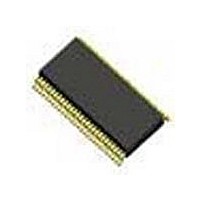
DS90CF383MTDX National Semiconductor, DS90CF383MTDX Datasheet - Page 3

DS90CF383MTDX
Manufacturer Part Number
DS90CF383MTDX
Description
Manufacturer
National Semiconductor
Datasheet
1.DS90CF383MTDX.pdf
(9 pages)
Specifications of DS90CF383MTDX
Number Of Elements
4
Number Of Receivers
28
Number Of Drivers
4
Input Type
CMOS/TTL
Operating Supply Voltage (typ)
3.3V
Differential Input High Threshold Voltage
100mV
Diff. Input Low Threshold Volt
-100mV
Output Type
Flat Panel Display
Differential Output Voltage
450mV
Power Dissipation
1.63W
Operating Temp Range
-40C to 85C
Operating Temperature Classification
Industrial
Mounting
Surface Mount
Pin Count
56
Package Type
TSSOP
Lead Free Status / Rohs Status
Not Compliant
Available stocks
Company
Part Number
Manufacturer
Quantity
Price
Company:
Part Number:
DS90CF383MTDX
Manufacturer:
ON
Quantity:
6 094
Part Number:
DS90CF383MTDX
Manufacturer:
NS/国半
Quantity:
20 000
Company:
Part Number:
DS90CF383MTDX/NOPB
Manufacturer:
NS
Quantity:
9 132
LLHT
LHLT
TCIT
TCCS
TPPos0
TPPos1
TPPos2
TPPos3
TPPos4
TPPos5
TPPos6
TCIP
TCIH
TCIL
TSTC
THTC
TCCD
TPLLS
TPDD
Symbol
Over recommended operating supply and temperature ranges unless otherwise specified
Electrical Characteristics
Note 2: Typical values are given for V
Note 3: Current into device pins is defined as positive. Current out of device pins is defined as negative. Voltages are referenced to ground unless otherwise speci-
fied (except V
Note 4: V
Transmitter Switching Characteristics
AC Timing Diagrams
OS
OD
previously referred as V
LVDS Low-to-High Transition Time (Figure 3 )
LVDS High-to-Low Transition Time (Figure 3 )
TxCLK IN Transition Time (Figure 4 )
TxOUT Channel-to-Channel Skew (Figure 5 )
Transmitter Output Pulse Position for Bit 0 (Figure 12 )
Transmitter Output Pulse Position for Bit 1
Transmitter Output Pulse Position for Bit 2
Transmitter Output Pulse Position for Bit 3
Transmitter Output Pulse Position for Bit 4
Transmitter Output Pulse Position for Bit 5
Transmitter Output Pulse Position for Bit 6
TxCLK IN Period (Figure 6)
TxCLK IN High Time (Figure 6)
TxCLK IN Low Time (Figure 6)
TxIN Setup to TxCLK IN (Figure 6)
TxIN Hold to TxCLK IN (Figure 6)
TxCLK IN to TxCLK OUT Delay 25˚C, V
Transmitter Phase Lock Loop Set (Figure 8 )
Transmitter Power Down Delay (Figure 11)
and V
OD
).
CM
CC
.
= 3.3V and T
(Continued)
A
FIGURE 1. “Worst Case” Test Pattern
= +25C.
Parameter
CC
= 3.3V (Figure 7 )
3
f = 65 MHz
f = 65 MHz
0.35T
0.35T
−0.4
10.6
12.8
Min
1.8
4.0
6.2
8.4
2.5
15
0
3
0.5T
0.5T
0.75
0.75
11.0
13.2
Typ
250
2.2
4.4
6.6
8.8
T
0
DS100033-4
0.65T
0.65T
www.national.com
Max
11.3
13.5
100
1.5
1.5
0.3
2.5
4.7
6.9
9.1
5.5
50
10
5
Units
ms
ns
ns
ns
ps
ps
ns
ns
ns
ns
ns
ns
ns
ns
ns
ns
ns
ns
ns


