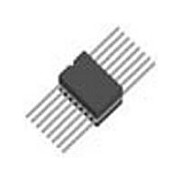
DS90LV031AWGQML National Semiconductor, DS90LV031AWGQML Datasheet

DS90LV031AWGQML
Specifications of DS90LV031AWGQML
Related parts for DS90LV031AWGQML
DS90LV031AWGQML Summary of contents
Page 1
... See NS Package Number M16A or MTC16 or W16A Truth Table DRIVER EN L All other combinations of ENABLE inputs TRI-STATE ® registered trademark of National Semiconductor Corporation. © 1999 National Semiconductor Corporation DS100095 Features > 400 Mbps (200 MHz) switching rates n n 0.1 ns typical differential skew n 0.4 ns maximum differential skew n 2 ...
Page 2
... Absolute Maximum Ratings If Military/Aerospace specified devices are required, please contact the National Semiconductor Sales Office/ Distributors for availability and specifications. Supply Voltage ( Input Voltage (D ) −0. Enable Input Voltage (EN −0. Output Voltage ( OUT+ OUT− Short Circuit Duration ( OUT+ OUT− @ Maximum Package Power Dissipation ...
Page 3
Switching Characteristics - Industrial = +3.3V ± = −40˚C to +85˚C (Notes 3, 9, 12 Symbol Parameter t Differential Propagation Delay High to Low PHLD t Differential Propagation Delay Low to High PLHD t Differential ...
Page 4
Parameter Measurement Information FIGURE 2. Driver Propagation Delay and Transition Time Test Circuit FIGURE 3. Driver Propagation Delay and Transition Time Waveforms FIGURE 4. Driver TRI-STATE Delay Test Circuit www.national.com FIGURE 1. Driver V and V Test Circuit OD OS ...
Page 5
Parameter Measurement Information FIGURE 5. Driver TRI-STATE Delay Waveform Typical Application Applications Information General application guidelines and hints for LVDS drivers and receivers may be found in the following application notes: LVDS Owner’s Manual (lit #550062-001), AN808, AN1035, AN977, AN971, ...
Page 6
Applications Information The TRI-STATE function allows the driver outputs to be dis- abled, thus obtaining an even lower power state when the transmission of data is not required. The footprint of the DS90LV031A is the same as the industry standard ...
Page 7
Applications Information (Continued) 3. Shorted Inputs fault condition occurs that shorts the receiver inputs together, thus resulting differ- ential input voltage, the receiver output will remain in a HIGH state. Shorted input fail-safe is not ...
Page 8
Applications Information FIGURE 9. Typical DS90LV031A, D www.national.com (Continued) DS100095- OUT 3.3V 25˚ ...
Page 9
Physical Dimensions inches (millimeters) unless otherwise noted 16-Lead (0.150" Wide) Molded Small Outline Package, JEDEC Order Number DS90LV031ATM NS Package Number M16A 9 www.national.com ...
Page 10
Physical Dimensions inches (millimeters) unless otherwise noted (Continued) 16-Lead (0.100" Wide) Molded Thin Shrink Small Outline Package, JEDEC www.national.com Order Number DS90LV031ATMTC NS Package Number MTC16 10 ...
Page 11
... NATIONAL’S PRODUCTS ARE NOT AUTHORIZED FOR USE AS CRITICAL COMPONENTS IN LIFE SUPPORT DEVICES OR SYSTEMS WITHOUT THE EXPRESS WRITTEN APPROVAL OF THE PRESIDENT AND GENERAL COUNSEL OF NATIONAL SEMICONDUCTOR CORPORATION. As used herein: 1. Life support devices or systems are devices or systems which, (a) are intended for surgical implant ...


