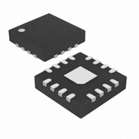
MAX13481EETE+T Maxim Integrated Products, MAX13481EETE+T Datasheet - Page 2

MAX13481EETE+T
Manufacturer Part Number
MAX13481EETE+T
Description
IC TXRX USB ESD PROT 16-TQFN
Manufacturer
Maxim Integrated Products
Type
Transceiverr
Datasheet
1.MAX13481EETET.pdf
(19 pages)
Specifications of MAX13481EETE+T
Number Of Drivers/receivers
1/1
Protocol
USB 2.0
Voltage - Supply
4 V ~ 5.5 V
Mounting Type
Surface Mount
Package / Case
16-TQFN Exposed Pad
Lead Free Status / RoHS Status
Lead free / RoHS Compliant
ABSOLUTE MAXIMUM RATINGS
(All voltages referenced to GND, unless otherwise noted.)
V
V
Input Voltage (D+, D-) ..............................................-0.3V to +7V
VM, VP, SUS, RCV,
Short-Circuit Current to V
Maximum Continuous Current (all other pins) ..................±15mA
±15kV ESD-Protected USB Transceivers with
External/Internal Pullup Resistors
ELECTRICAL CHARACTERISTICS
(V
T
Stresses beyond those listed under “Absolute Maximum Ratings” may cause permanent damage to the device. These are stress ratings only, and functional
operation of the device at these or any other conditions beyond those indicated in the operational sections of the specifications is not implied. Exposure to
absolute maximum rating conditions for extended periods may affect device reliability.
2
SUPPLY INPUTS (V
V
V
Regulated Supply-Voltage Output
Operating V
Operating V
Full-Speed Idle and SE0 Supply
Current
Static V
Suspend Supply Current
Disabled-Mode Supply Current
Sharing-Mode V
Disable-Mode Load Current on
D+ and D-
Sharing-Mode Load Current on
D+ and D-
USB Power-Supply Detection
Threshold
USB Power-Supply Detection
Hysteresis
V
Threshold
BUS
TRM
A
CC
BUS
L
L
= +25°C.) (Note 1)
Input Range
Supply-Voltage Detection
_______________________________________________________________________________________
, V
, VPUR, VPU .....................................-0.3V to (V
= +4V to +5.5V, V
Input Range
L,
L
..................................................................-0.3V to +7V
Supply Current
PARAMETER
CC
L
Supply Current
Supply Current
L
Supply Current
ENUM, BD, OE, ............-0.3V to (V
BUS
L
CC
= +1.6V to +3.6V, T
, V
or GND (D+, D-)… ........... ±150mA
TRM
, V
L
)
I
I
I
DX (SH ARING)
I
I
V L(S H ARIN G)
D X (D IS ABLE )
I
SYMBOL
VL(STATIC)
VCC(SUSP)
VCC(IDLE)
I
VCC(DIS)
V
V
V
V
V
V
I
TH(VL)
VTRM
VCC
TH_H
HYST
TH_L
I
BUS
V
VL
L
A
= T
Full-speed transmitting/receiving at
12Mbps, C
Full-speed transmitting/receiving at
12Mbps, C
V
Full-speed idle, V
SE0: V
Full-speed idle, SE0 or suspend mode
VM = VP = open, ENUM = SUS = OE = high
V
V
VP = low or high, VM = low or high, SUS =
high, ENUM = high
V
V
Supply present
Supply lost
MIN
L
L
BUS
L
BUS
BUS
= 2.5V (Note 2)
= GND or open
= GND or open, V
L
to T
= GND or open, OE = low,
= GND or open, V
+ 0.3V)
+ 0.3V)
D+
MAX
< 0.3V, V
L
L
, unless otherwise noted. Typical values are at V
= 50pF on D+ and D- (Note 2)
= 15pF receiver outputs,
CONDITIONS
D+
D-
Continuous Power Dissipation (T
Operating Temperature Range ...........................-40°C to +85°C
Junction Temperature ......................................................+150°C
Storage Temperature Range .............................-65°C to +150°C
Lead Temperature (soldering, 10s) .................................+300°C
> 2.7V, V
D_
< 0.3V
16-Pin, 3mm x 3mm TQFN (derate 15.6mW/°C above
+70°C).......................................................................1250mW
V
V
D_
= 0 or 5.5V
L
L
≥ 1.7V
< 1.7V
= 0 or 5.5V
D-
< 0.3V
MIN
4.0
1.6
3.0
3.6
A
= +70°C)
TYP
0.85
250
250
3.3
75
CC
= +5V, V
MAX
350
350
5.5
3.6
3.6
2.5
0.8
0.7
10
35
20
20
5
5
5
L
= +2.5V,
UNITS
mA
mA
mV
µA
µA
µA
µA
µA
µA
µA
V
V
V
V
V


