Si5327-EVB Silicon Laboratories Inc, Si5327-EVB Datasheet - Page 5
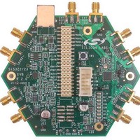
Si5327-EVB
Manufacturer Part Number
Si5327-EVB
Description
MCU, MPU & DSP Development Tools SI5327 EVAL BOARD
Manufacturer
Silicon Laboratories Inc
Specifications of Si5327-EVB
Processor To Be Evaluated
Si5327
Interface Type
I2C, SPI
Operating Supply Voltage
3.3 V
Lead Free Status / Rohs Status
Details


Table 2 shows how the various components should be configured for the three modes of operation.
For a differential external reference, connect the balanced input signals to J1 and J2. For single-ended operation,
connect the input signal to J2 and disconnect J1.
R35 is provided so that a different termination scheme can be used. If R35 is populated, then remove R9 and R36.
5.4. Two and Three Level Inputs
The two-level and three-level inputs can all be manually configured by installing jumper plugs at J9. The two level
inputs are either H or L. For the three-level inputs, the M level is achieved by not installing a jumper plug at a given
location. J9 can also be used as a connection to an external circuit that controls these pins. J17 is a ten pin ribbon
header that is provided so that an external processor can control the Si532x over either the SPI or I
J14 is another ten pin ribbon header that brings out all of the status outputs from the Si532x. Note that some pins
are shared and serve as both inputs and outputs, depending on how the device is configured. For users that wish
to remotely access the input and output pins settings as well as serial ports with external hardware, all three of
these headers can be connected to ribbon cables.
5.5. CPLD and Power
This CPLD is required for the MCU to control the Si532x. The CPLD provides two main functions: it translates the
voltage level from 3.3 V (the MCU voltage) to the Si532x voltage (either 1.8, 2.5, or 3.3 V). The MCU
communicates to the CPLD with the SPI signals SS_CPLD_B (slave select), MISO (master in, slave out), MOSI
(master out, slave in), and SCLK. The MCU can talk to CPLD-resident registers that are connected to pins that
control the Si532x's pins, mainly for pin control mode. When the MCU wishes to access a Si532x register, the SPI
signals are passed through the CPLD, while being level translated, to the Si532x. The CPLD is an EE device that
retains its code and is loaded through the JTAG port (J27). The core of the CPLD runs at 1.8 V, which is provided
by voltage regulator U6. The CPLD also logically connects many of the LEDs to the appropriate Si532x pins.
Notes:
1. Xtal is 114.285 MHz third overtone; 40 MHz fundamental for the
2. For external reference frequencies and RATE pin settings, see the
3. NC—No connect.
4. NOPOP—Do not install this component.
5. RATE options for Si5327 only.
Input 1
Input 2
RATE0
RATE1
RATE
C30
R34
R15
C5
Si5327-EVB
Si53xx-RM Any-Frequency Precision Clock Family
Reference Manual
5
Table 2. Reference Input Mode
NOPOP
NOPOP
NOPOP
install
Xtal
NC
NC
M
M
L
3
1
.
4
Rev. 0.5
Ext Ref
NOPOP
NOPOP
Mode
install
install
NC
J1
J2
—
—
2
Wide Band
NOPOP
NOPOP
install
install
NC
NC
—
H
H
Si531x-EVB
Si532x-EVB
2
C bus.
5
Related parts for Si5327-EVB
Image
Part Number
Description
Manufacturer
Datasheet
Request
R

Part Number:
Description:
SMD/C°/SINGLE-ENDED OUTPUT SILICON OSCILLATOR
Manufacturer:
Silicon Laboratories Inc
Part Number:
Description:
Manufacturer:
Silicon Laboratories Inc
Datasheet:
Part Number:
Description:
N/A N/A/SI4010 AES KEYFOB DEMO WITH LCD RX
Manufacturer:
Silicon Laboratories Inc
Datasheet:
Part Number:
Description:
N/A N/A/SI4010 SIMPLIFIED KEY FOB DEMO WITH LED RX
Manufacturer:
Silicon Laboratories Inc
Datasheet:
Part Number:
Description:
N/A/-40 TO 85 OC/EZLINK MODULE; F930/4432 HIGH BAND (REV E/B1)
Manufacturer:
Silicon Laboratories Inc
Part Number:
Description:
EZLink Module; F930/4432 Low Band (rev e/B1)
Manufacturer:
Silicon Laboratories Inc
Part Number:
Description:
I°/4460 10 DBM RADIO TEST CARD 434 MHZ
Manufacturer:
Silicon Laboratories Inc
Part Number:
Description:
I°/4461 14 DBM RADIO TEST CARD 868 MHZ
Manufacturer:
Silicon Laboratories Inc
Part Number:
Description:
I°/4463 20 DBM RFSWITCH RADIO TEST CARD 460 MHZ
Manufacturer:
Silicon Laboratories Inc
Part Number:
Description:
I°/4463 20 DBM RADIO TEST CARD 868 MHZ
Manufacturer:
Silicon Laboratories Inc
Part Number:
Description:
I°/4463 27 DBM RADIO TEST CARD 868 MHZ
Manufacturer:
Silicon Laboratories Inc
Part Number:
Description:
I°/4463 SKYWORKS 30 DBM RADIO TEST CARD 915 MHZ
Manufacturer:
Silicon Laboratories Inc
Part Number:
Description:
N/A N/A/-40 TO 85 OC/4463 RFMD 30 DBM RADIO TEST CARD 915 MHZ
Manufacturer:
Silicon Laboratories Inc
Part Number:
Description:
I°/4463 20 DBM RADIO TEST CARD 169 MHZ
Manufacturer:
Silicon Laboratories Inc