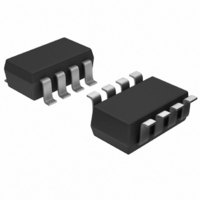
MAX9111EKA+T Maxim Integrated Products, MAX9111EKA+T Datasheet - Page 2

MAX9111EKA+T
Manufacturer Part Number
MAX9111EKA+T
Description
IC RCVR SNGL LVDS SOT23-8
Manufacturer
Maxim Integrated Products
Type
Receiverr
Specifications of MAX9111EKA+T
Number Of Drivers/receivers
0/1
Protocol
LVDS
Voltage - Supply
3 V ~ 3.6 V
Mounting Type
Surface Mount
Package / Case
SOT-23-8
Logic Family
MAX9111
Logic Type
LVDS Line Receiver
Supply Voltage (max)
4 V
Supply Voltage (min)
- 0.3 V
Maximum Operating Temperature
+ 85 C
Mounting Style
SMD/SMT
Data Rate
500 Mbps
Maximum Power Dissipation
714 mW
Minimum Operating Temperature
- 40 C
Output Voltage
+/- 0.3 V
Propagation Delay Time
1.77 ns
Supply Current
4.2 mA
Lead Free Status / RoHS Status
Lead free / RoHS Compliant
Single/Dual LVDS Line Receivers with
Ultra-Low Pulse Skew in SOT23
ABSOLUTE MAXIMUM RATINGS
V
IN_ _ to GND .........................................................-0.3V to +3.9V
OUT_ _ to GND...........................................-0.3V to (V
ESD Protection All Pins
Continuous Power Dissipation (T
Stresses beyond those listed under “Absolute Maximum Ratings” may cause permanent damage to the device. These are stress ratings only, and functional
operation of the device at these or any other conditions beyond those indicated in the operational sections of the specifications is not implied. Exposure to
absolute maximum rating conditions for extended periods may affect device reliability.
ELECTRICAL CHARACTERISTICS
(V
Typical values are at V
2
CC
Differential Input High Threshold
(Note 3)
Differential Input Low Threshold
(Note 3)
Differential Input Resistance
Output High Voltage (OUT_)
Output Low Voltage (OUT_)
Output Short-Circuit Current
No-Load Supply Current
CC
(Human Body Model, IN_+, IN_-) ..................................±11kV
8-Pin SOT23 (derate 8.9mW/°C above +70°C)............714mW
_______________________________________________________________________________________
to GND ..............................................................-0.3V to +4V
= +3.0V to +3.6V, magnitude of input voltage, |V
PARAMETER
CC
= +3.3V and T
A
= +70°C)
SYMBOL
R
V
V
V
V
I
I
DIFF
OS
CC
A
OH
TH
OL
TL
= +25°C, unless otherwise noted.) (Notes 1, 2)
V
V
I
I
V
MAX9111
MAX9113
V
V
OH
OL
CM
CC
ID
CM
CM
CC
= 4mA, V
= -4mA
= +200mV, V
= 0 or 3.6V
= 0.2V or 2.2V, V
= 0.05V, 1.2V, 2.75V at 3.3V
= 0.05V, 1.2V, 2.75V at 3.3V
+ 0.3V)
ID
| = +0.1V to +1.0V, V
ID
CONDITIONS
= -200mV
OUT
Operating Temperature Ranges
Storage Temperature Range .............................-65°C to +150°C
Lead Temperature (soldering, 10s) .................................+300°C
_ = 0
ID
8-Pin SO (derate 5.88mW°C above +70°C).................471mW
MAX911_E .......................................................-40°C to +85°C
MAX911_A .....................................................-40°C to +125°C
= ±0.4V,
V
Inputs shorted,
undriven
100Ω parallel
termination,
undriven
ID
= +200mV
CM
= |V
ID
|/2 to (2.4V - (|V
-100
MIN
2.7
2.7
2.7
5
ID
TYP
|/2)), T
4.2
8.7
18
A
MAX
-100
= T
100
0.4
11
6
MIN
to T
UNITS
mA
mV
mV
mA
kΩ
V
MAX
.


