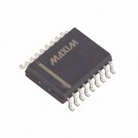
MAX563CWN Maxim Integrated Products, MAX563CWN Datasheet - Page 5

MAX563CWN
Manufacturer Part Number
MAX563CWN
Description
IC TXRX RS232 DUAL 3.3V 18-SOIC
Manufacturer
Maxim Integrated Products
Type
Transceiverr
Datasheet
1.MAX563CWN.pdf
(8 pages)
Specifications of MAX563CWN
Number Of Drivers/receivers
2/2
Protocol
RS562
Voltage - Supply
3 V ~ 3.6 V
Mounting Type
Surface Mount
Package / Case
18-SOIC (7.5mm Width)
Lead Free Status / RoHS Status
Contains lead / RoHS non-compliant
Available stocks
Company
Part Number
Manufacturer
Quantity
Price
Part Number:
MAX563CWN
Manufacturer:
MAXIM/美信
Quantity:
20 000
Company:
Part Number:
MAX563CWN+
Manufacturer:
Microchip
Quantity:
434
Figure 1. Shutdown Current Test Circuit
The inputs of unused drivers may be left unconnected
because they have internal 400kΩ pull-ups to V
Unused inputs may also be connected to GND or V
but V
the internal pull-ups.
The MAX563’s receivers convert ±3.7V to ±13.2V
EIA/TIA-562 signal levels into +3V logic levels; they are
rated to receive signals up to ±25V to accommodate
EIA/TIA-232 signals as well. Both receivers invert. Their
inputs are each equipped with an internal 5kΩ (nomi-
nal) terminating resistor connected to ground, and the
input logic thresholds are 0.4V and 2.4V. The positive
logic-low threshold (V
remain high whenever their inputs are left open.
The receivers are active when EN is low, and have
high-impedance outputs when EN is high.
When SHDN is high, the receivers have hysteresis.
This produces clean output transitions, even with slow-
moving input signals that exhibit moderate amounts of
noise and ringing. When shut down, the receivers have
no hysteresis, and the propagation delay increases.
The SHDN and EN controls are independent. Both
receivers are always active when EN is low. With EN
low and SHDN high, the receivers operate at full speed
CC
EIA/TIA-562 and EIA/TIA-232 Receivers
0V +3.6V
+3.3V-Powered, EIA/TIA-562 Dual Transceiver
+3.6V
DRIVE
0.1µF
0.1µF
0.1µF
provides lower power consumption because of
+3.6V
Shutdown and Enable Control
I
SHDN
_______________________________________________________________________________________
C1+
C1-
C2+
C2-
T
R
EN
SHDN
IN
OUT
V
IL
CC
R1 & R2
) ensures the receiver outputs
400k
MAX563
GND
V
T1 & T2
CC
with Receivers Active in Shutdown
T
OUT
R
5k
V+
V-
IN
0.1µF
0.1µF
+3.6V
3k
CC
CC
.
,
and have hysteresis. When active in shutdown mode
(EN = SHDN = low), the receivers operate at reduced
power and speed, and without hysteresis.
The charge pumps and transmitters operate only when
SHDN is high; they are unaffected by EN. When shut
down (SHDN = low) or unpowered (V
transmitter outputs are high impedance if they are
backdriven with voltages not exceeding ±15V. The pull-
up resistors at the driver inputs are disconnected in
shutdown mode to save power. During shutdown, V+ is
pulled down to V
Figure 2. Transmitter Propagation Delay Timing
Figure 3. Receiver Propagation Delay Timing
OUTPUT
INPUT
OUTPUT
INPUT
t
t
+3V
PHLR
PHLS
t
PLHT
CC
, and V- rises to GND.
50%
50%
+3V
OV
CC
50%
50%
GND
= 0V), the
t
t
t
PLHR
PLHS
PHLT
V
OV
0V
V+
V-
CC
5


