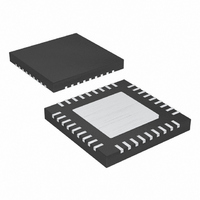
MAX4950ACTX+T Maxim Integrated Products, MAX4950ACTX+T Datasheet

MAX4950ACTX+T
Specifications of MAX4950ACTX+T
Related parts for MAX4950ACTX+T
MAX4950ACTX+T Summary of contents
Page 1
... Three-Level Programmable Input Equalization ♦ Three-Level Programmable Output Deemphasis ♦ Standard, -2.5dB Programmable Output Levels ♦ On-Chip 50Ω Input/Output Terminations ♦ Space-Saving, 6.0mm x 6.0mm TQFN Package Applications PART MAX4950ACTX+T + Denotes a lead(Pb)-free/RoHS-compliant package Exposed pad Tape and reel. TOP VIEW N.C. 28 ...
Page 2
Dual PCI Express Equalizer/Redriver ABSOLUTE MAXIMUM RATINGS (Voltages referenced to GND.) V ........................................................................-0.3V to +4.0V CC All Other Pins (Note 1)................................-0. Continuous Current IN_P, IN_M, OUT_P, OUT_M ............±30mA Peak Current IN_P, IN_M, OUT_P, OUT_M (pulsed for 1µs, 1% ...
Page 3
Dual PCI Express Equalizer/Redriver ELECTRICAL CHARACTERISTICS (continued +3.0V to +3.6V 75nF coupling capacitor on each output otherwise noted. Typical values are at V PARAMETER SYMBOL Differential Output Return Loss RL (Note 5) Common-Mode ...
Page 4
Dual PCI Express Equalizer/Redriver ELECTRICAL CHARACTERISTICS (continued +3.0V to +3.6V 75nF coupling capacitor on each output otherwise noted. Typical values are at V PARAMETER SYMBOL V TX-IDLE- Electrical Idle Detect Threshold THRESH Output ...
Page 5
Dual PCI Express Equalizer/Redriver (V = +3.3V +25°C, unless otherwise noted INEQ_0 = INEQ_1 = 0, O_AMP_ = 200mV , ODE_0 = 0, ODE_1 = 0 IN P-P 600 400 200 0 -200 ...
Page 6
Dual PCI Express Equalizer/Redriver (V = +3.3V +25°C, unless otherwise noted INEQ_0 = 1, INEQ_1 = 0, O_AMP_ = 0, V WITH 6in STRIPLINE ODE_0 = ODE_1 = 0 600 400 200 0 -200 -400 -600 ...
Page 7
Dual PCI Express Equalizer/Redriver PIN NAME 19, GND Ground 22, 24 INAP Noninverting Input A 3 INAM Inverting Input A Enable Input. Drive EN low for standby mode. Drive EN high for normal mode. ...
Page 8
Dual PCI Express Equalizer/Redriver MAX4950A INEQ_0 INEQ_1 IN_P IN_M EQUALIZER R HI ELECTRICAL IDLE DETECTOR Figure 2. Block Diagram of Each Channel 8 _______________________________________________________________________________________ EN RX_DET O_AMP_ GLOBAL POWER SAVE RECEIVER DETECT MANAGER EQUALIZER ODE_0 ODE_1 OUT_P OUT_M ...
Page 9
Dual PCI Express Equalizer/Redriver Detailed Description The MAX4950A dual equalizer/redriver is designed to support both Gen I (2.5GT/s) and Gen II (5.0GT/s) PCIe data rates. The device contains two identical drivers with idle/receive detect on each lane and equalization to ...
Page 10
... Maxim cannot assume responsibility for use of any circuitry other than circuitry entirely embodied in a Maxim product. No circuit patent licenses are implied. Maxim reserves the right to change the circuitry and specifications without notice at any time. 10 ____________________Maxim Integrated Products, 120 San Gabriel Drive, Sunnyvale, CA 94086 408-737-7600 © 2009 Maxim Integrated Products ...


