BSP52T ON Semiconductor, BSP52T Datasheet

BSP52T

Manufacturer Part Number
BSP52T
Description
Manufacturer
ON Semiconductor
Datasheet

Specifications of BSP52T

Polarity
NPN
Number Of Elements
1
Collector-emitter Voltage
80V
Collector-base Voltage
90V
Emitter-base Voltage
5V
Base-emitter Saturation Voltage (max)
1.9V
Collector-emitter Saturation Voltage
1.3V
Collector Current (dc) (max)
1A
Dc Current Gain
1000
Operating Temp Range
-65C to 150C
Operating Temperature Classification
Military
Mounting
Surface Mount
Pin Count
3 +Tab
Package Type
SOT-223
Lead Free Status / Rohs Status
Not Compliant

Available stocks

Company
Part Number
Manufacturer
Quantity
Price
Part Number:
BSP52T1G
Manufacturer:
ON
Quantity:
5 000
Part Number:
BSP52T1G
Manufacturer:
ON Semiconductor
Quantity:
152
Part Number:
BSP52T1G
Manufacturer:
ON
Quantity:
12 500
Part Number:
BSP52T1G
Manufacturer:
ON
Quantity:
4 000
Part Number:
BSP52T1G
0
Company:
Part Number:
BSP52T1G
Quantity:
4 500
Part Number:
BSP52T3G
Manufacturer:
ON
Quantity:
12 500
BSP52T1, BSP52T3
NPN Small−Signal
Darlington Transistor
switching applications, such as print hammer, relay, solenoid and lamp
drivers. The device is housed in the SOT-223 package, which is
designed for medium power surface mount applications.
Features
1. Device mounted on a FR-4 glass epoxy printed circuit board using minimum
2. Device mounted on a FR-4 glass epoxy printed circuit board using 1 cm
THERMAL CHARACTERISTICS
© Semiconductor Components Industries, LLC, 2005
September, 2005 − Rev. 5
MAXIMUM RATINGS
Maximum ratings are those values beyond which device damage can occur.
Maximum ratings applied to the device are individual stress limit values (not
normal operating conditions) and are not valid simultaneously. If these limits
are exceeded, device functional operation is not implied, damage may occur
and reliability may be affected.
Collector-Emitter Voltage
Collector-Base Voltage
Emitter-Base Voltage
Collector Current
Total Power Dissipation (Note 1)
Total Power Dissipation (Note 2)
Operating and Storage
Thermal Resistance (Note 1)
Thermal Resistance (Note 2)
Maximum Temperature for Soldering
This NPN small signal Darlington transistor is designed for use in
formed leads absorb thermal stress during soldering, eliminating the
possibility of damage to the die
Use BSP52T1 to order the 7 inch/1000 unit reel
The SOT-223 Package can be soldered using wave or reflow. The
Available in 12 mm Tape and Reel
PNP Complement is BSP62T1
Pb−Free Packages are Available
recommended footprint.
@ T
Derate above 25°C
@ T
Derate above 25°C
Temperature Range
Junction-to-Ambient
Junction-to-Ambient
Purposes
Time in Solder Bath
A
A
= 25°C
= 25°C
Characteristic
Rating
(T
C
Preferred Devices
= 25°C unless otherwise noted)
Symbol
Symbol
T
V
V
V
R
R
J
P
P
CBO
EBO
, T
T
CES
I
qJA
qJA
C
D
D
L
stg
−65 to 150
Value
Max
1.25
156
100
260
5.0
1.0
0.8
6.4
80
90
10
10
1
mW/°C
mW/°C
°C/W
°C/W
Unit
Unit
Vdc
Vdc
Vdc
Adc
Sec
°C
°C
W
W
2
pad.
†For information on tape and reel specifications,
Preferred devices are recommended choices for future use
and best overall value.
BSP52T1G
BSP52T3G
BSP52T1
BSP52T3
including part orientation and tape sizes, please
refer to our Tape and Reel Packaging Specifications
Brochure, BRD8011/D.
DARLINGTON TRANSISTOR
Device
CASE 318E
1
SOT−223
STYLE 1
A
Y
W
AS3
G
(Note: Microdot may be in either location)
2
ORDERING INFORMATION
SURFACE MOUNT
3
MEDIUM POWER
http://onsemi.com
NPN SILICON
= Assembly Location
= Year
= Work Week
= Specific Device Code
= Pb−Free Package
4
(Pb−Free)
(Pb−Free)
SOT−223
SOT−223
SOT−223
SOT−223
Package
BASE
1
COLLECTOR 2,4
EMITTER 3
Publication Order Number:
MARKING DIAGRAM
1000/Tape & Reel
1000/Tape & Reel
4000/Tape & Reel
4000/Tape & Reel
Shipping
AS3G
AYW
G
BSP52T1/D

Related parts for BSP52T

BSP52T Summary of contents

Page 1

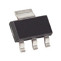
... The SOT-223 Package can be soldered using wave or reflow. The formed leads absorb thermal stress during soldering, eliminating the possibility of damage to the die • Available Tape and Reel Use BSP52T1 to order the 7 inch/1000 unit reel • PNP Complement is BSP62T1 • Pb−Free Packages are Available ...

Page 2

... C CE Collector-Emitter Saturation Voltage (I = 500 mAdc 0.5 mAdc Base-Emitter Saturation Voltage (I = 500 mAdc 0.5 mAdc Pulse Test: Pulse Width ≤ 300 ms, Duty Cycle ≤ 2.0% BSP52T1, BSP52T3 (T = 25°C unless otherwise noted) A http://onsemi.com 2 Symbol Min Max Unit V Vdc (BR)CBO 90 − ...

Page 3

... A 0.08 (0003) A1 2.0 0.079 *For additional information on our Pb−Free strategy and soldering details, please download the ON Semiconductor Soldering and Mounting Techniques Reference Manual, SOLDERRM/D. BSP52T1, BSP52T3 PACKAGE DIMENSIONS SOT−223 CASE 318E−04 ISSUE L NOTES: 1. DIMENSIONING AND TOLERANCING PER ANSI Y14.5M, 1982. ...

Page 4

... P.O. Box 61312, Phoenix, Arizona 85082−1312 USA Phone: 480−829−7710 or 800−344−3860 Toll Free USA/Canada Fax: 480−829−7709 or 800−344−3867 Toll Free USA/Canada Email: orderlit@onsemi.com BSP52T1, BSP52T3 N. American Technical Support: 800−282−9855 Toll Free USA/Canada Japan: ON Semiconductor, Japan Customer Focus Center 2− ...

Related keywords