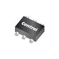
CMRDM3575 Central Semiconductor, CMRDM3575 Datasheet

CMRDM3575
Manufacturer Part Number
CMRDM3575
Description
MOSFET Small Signal N AND P CHANNEL MOSFET
Manufacturer
Central Semiconductor
Datasheet
1.CMRDM3575.pdf
(2 pages)
Specifications of CMRDM3575
Configuration
Single
Transistor Polarity
N and P-Channel
Resistance Drain-source Rds (on)
1.5 Ohms, 4 Ohms
Forward Transconductance Gfs (max / Min)
1.3 S
Drain-source Breakdown Voltage
20 V
Continuous Drain Current
160 mA, 140 mA
Power Dissipation
125 mW
Maximum Operating Temperature
+ 150 C
Mounting Style
SMD/SMT
Package / Case
SOT-963
Minimum Operating Temperature
- 65 C
Lead Free Status / Rohs Status
Details
• Device is Halogen Free by design
APPLICATIONS:
• Load/Power Switches
• Power Supply Converter Circuits
• Battery Powered Portable Devices
MAXIMUM RATINGS: (T A =25°C)
Drain-Source Voltage
Gate-Source Voltage
Continuous Drain Current (Steady State)
Continuous Drain Current, t p < 5.0s
Power Dissipation
Operating and Storage Junction Temperature
Thermal Resistance
ELECTRICAL CHARACTERISTICS: (T A =25°C)
SYMBOL
I GSSF , I GSSR V GS =5.0V, V DS =0
I DSS
I DSS
BV DSS
V GS(th)
r DS(ON)
r DS(ON)
r DS(ON)
r DS(ON)
r DS(ON)
g FS
C rss
C iss
C oss
t on
t off
COMPLEMENTARY SILICON MOSFETS
N-CHANNEL AND P-CHANNEL
ENHANCEMENT-MODE
SURFACE MOUNT
SOT-963 CASE
TEST CONDITIONS
V DS =5.0V, V GS =0
V DS =16V, V GS =0
V GS =0, I D =250μA
V DS =V GS, I D =250μA
V GS =4.5V, I D =100mA
V GS =2.5V, I D =50mA
V GS =1.8V, I D =20mA
V GS =1.5V, I D =10mA
V GS =1.2V, I D =1.0mA
V DS =5.0V, I D =125mA
V DS =15V, V GS =0, f=1.0MHz
V DS =15V, V GS =0, f=1.0MHz
V DS =15V, V GS =0, f=1.0MHz
V DD =10V, V GS =4.5V, I D =200mA
V DD =10V, V GS =4.5V, I D =200mA
CMRDM3575
MIN TYP MAX
0.4
20
DESCRIPTION:
The CENTRAL SEMICONDUCTOR CMRDM3575
consists of complementary N-Channel and P-Channel
Enhancement-mode silicon MOSFETs designed for
high speed pulsed amplifier and driver applications.
These MOSFETs offer Low r DS(ON) and Low
Threshold Voltage.
MARKING CODE: CT
FEATURES:
• Power Dissipation: 125mW
• Low Package Profile: 0.5mm (MAX)
• Low r DS(ON)
• Low Threshold Voltage
• Logic Level Compatible
• Small SOT-963 Surface Mount Package
-
-
-
-
-
-
-
-
-
-
-
-
-
-
N-CH (Q1)
SYMBOL
T J , T stg
V DS
V GS
Θ JA
150
P D
1.5
2.0
3.0
4.0
7.0
1.3
2.2
9.0
3.0
40
I D
I D
-
-
-
-
-
100
100
1.0
3.0
4.0
6.0
50
10
-
-
-
-
-
-
-
-
N-CH (Q1)
160
200
-65 to +150
MIN TYP MAX
0.4
20
-
-
-
-
-
-
-
-
-
-
-
-
-
-
1000
125
8.0
20
P-CH (Q2)
P-CH (Q2)
210
4.0
5.5
8.0
1.3
1.0
2.7
11
20
12
60
-
-
-
-
-
140
180
w w w. c e n t r a l s e m i . c o m
100
100
1.0
5.0
7.0
50
10
17
-
-
-
-
-
-
-
-
R1 (8-February 2010)
UNITS
UNITS
°C/W
mW
mA
mA
nA
nA
nA
°C
pF
pF
pF
ns
ns
V
V
V
V
Ω
Ω
Ω
Ω
Ω
S
Related parts for CMRDM3575
CMRDM3575 Summary of contents
Page 1
... V DD =10V =4.5V =200mA t off V DD =10V =4.5V =200mA DESCRIPTION: The CENTRAL SEMICONDUCTOR CMRDM3575 consists of complementary N-Channel and P-Channel Enhancement-mode silicon MOSFETs designed for high speed pulsed amplifier and driver applications. These MOSFETs offer Low r DS(ON) and Low Threshold Voltage. MARKING CODE: CT FEATURES: • ...
Page 2
... CMRDM3575 SURFACE MOUNT N-CHANNEL AND P-CHANNEL ENHANCEMENT-MODE COMPLEMENTARY SILICON MOSFETS SOT-963 CASE - MECHANICAL OUTLINE PIN CONFIGURATION LEAD CODE: 1) Source Q1 2) Gate Q1 3) Drain Q2 4) Source Q2 5) Gate Q2 6) Drain Q1 MARKING CODE (8-February 2010) ...

