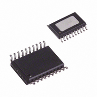
AD8016ARP-REEL Analog Devices Inc, AD8016ARP-REEL Datasheet

AD8016ARP-REEL
Specifications of AD8016ARP-REEL
Available stocks
Related parts for AD8016ARP-REEL
AD8016ARP-REEL Summary of contents
Page 1
FEATURES xDSL Line Driver that Features Full ADSL CO (Central Office) Performance Supplies Low Power Operation Voltage Supply 12.5 mA/Amp (Typ) Total Supply Current Power Reduced Keep Alive Current of 4.5 ...
Page 2
AD8016–SPECIFICATIONS Parameter DYNAMIC PERFORMANCE –3 dB Bandwidth Bandwidth for 0.1 dB Flatness Large Signal Bandwidth Peaking Slew Rate Rise and Fall Time Settling Time Input Overdrive Recovery Time NOISE/DISTORTION PERFORMANCE Distortion, Single-Ended Second Harmonic Third Harmonic Multitone Power Ratio* IMD ...
Page 3
C, V SPECIFICATIONS T MAX Parameter DYNAMIC PERFORMANCE –3 dB Bandwidth Bandwidth for 0.1 dB Flatness Large Signal Bandwidth Peaking Slew Rate Rise and Fall Time Settling Time Input Overdrive Recovery Time NOISE/DISTORTION PERFORMANCE Distortion, Single-Ended Second Harmonic ...
Page 4
... Specification is for device on a 4-layer board with 10 inches 24-lead Batwing package: θ = 28°C/ Specification is for device on a 4-layer board with 9 inches 28-lead (TSSOP-EP) package: θ = 29°C/W. JA Model AD8016ARP AD8016ARP-REEL AD8016ARP-EVAL AD8016ARB AD8016ARB-REEL AD8016ARB-EVAL AD8016ARE AD8016ARE-REEL AD8016ARE-REEL7 AD8016ARE-EVAL CAUTION ESD (electrostatic discharge) sensitive device. Electrostatic charges as high as 4000 V readily accumulate on the human body and test equipment and can discharge without detection ...
Page 5
V IN 49.9 0.1 F 0.1 F Figure 3. Single-Ended Test Circuit 100mV OUT V = 20mV IN TIME (100ns/DIV) Figure 4. 100 mV Step Response + Ω ...
Page 6
AD8016 – 499 F – + p-p O –50 –60 –70 –80 –90 –100 –110 0.01 0.1 1 FREQUENCY (MHz) Figure 9. Distortion vs. Frequency; Second Harmonic, = ± ...
Page 7
R = 499 F – –40 –45 (0,0) –50 (0,1) –55 –60 –65 –70 –75 –80 0 100 200 300 PEAK OUTPUT CURRENT (mA) Figure 15. Distortion vs. Peak Output Current; Second = ± ...
Page 8
AD8016 3 0 – 40mV p-p IN – 100 –9 L –12 –15 –18 –21 –24 – FREQUENCY (MHz) Figure 21. Frequency Response PWDN1, PWDN0 Codes ...
Page 9
NOISE NOISE 100 1k 10k FREQUENCY (MHz) Figure 27. Noise vs. Frequency +2mV (–0.1%) 0 –2mV (–0.1 OUT V OUT – ...
Page 10
AD8016 V OUT –100 0 100 200 300 400 500 TIME (ns) Figure 33a. Overload Recovery 100 Ω + OUT –100 0 100 200 300 ...
Page 11
THEORY OF OPERATION The AD8016 is a current feedback amplifier with high (500 mA) output current capability. With a current feedback amplifier, the current into the inverting input is the feedback signal and the open-loop behavior is that of a ...
Page 12
... Figure 39. Shutdown and Alarm Circuit ). A typical shut- APPLICATIONS Q The AD8016ARP and AD8016ARB dual xDSL line driver amplifiers are the most efficient xDSL line drivers available on the market today. The AD8016 may be applied in driving modu- lated signals including discrete multitone (DMT) in either direction ...
Page 13
... MTPR performance, sufficient for use in evaluating xDSL drivers. Note that the DMT waveforms available with the AD8016ARP-EVAL and AD8016ARB-EVAL boards or similar WFM files are needed to produce the neces- sary digital data required to drive the TxDAC from the optional TTL digital data output of the TEK AWG2021 ...
Page 14
... AD8016ARB or SO-Batwing package is 8.6°C/W, for JC the AD8016ARE or TSSOP- 5.6°C/W, and for the AD8016ARP or PSOP3 package it is 0.86°C/W. These package specifications were used in this study to determine junction temperature based on the measured case temperature. PCB Dimensions of a Differential Driver Circuit: Several components are required to support the AD8016 in a differential driver circuit ...
Page 15
EXPERIMENTAL RESULTS The experimental data suggests that for both packages, and a PCB as small as 4.7 square inches, reasonable junction tempera- tures can be maintained even in the absence of air flow. The graph in Figure 42 shows junction ...
Page 16
AD8016 Figure 45. DMT Signal Generator Schematic –16– REV. B ...
Page 17
TP10 TP5 AGND3,4 R11 R13 JP6 R23 1 JP5 AGND3,4,5 R14 S6 R16 R15 C10 TP11 TP4 ...
Page 18
AD8016 LAYOUT AD8016ARB-EVAL Figure 47. Assembly Figure 48. Layer 1 Figure 49. Power/Ground Plane Figure 50. Layer 1 Figure 51. Silkscreen Bottom –18– REV. B ...
Page 19
ALP – EVALUATION BOARD – BILL OF MATERIALS Quantity Description 10 µ Size Tantalum Chip Capacitor 5 0.1 µ 1206 Size Ceramic Chip Capacitor 10 49.9 Ω 1% 1/8 W 1206 Size Chip Resistor 2 100 ...
Page 20
AD8016 20-Lead Power SOIC, Thermally Enhanced Package [PSOP3] 11.00 BSC 3.60 3.35 3.10 SEATING PLANE 28-Lead Thin Shrink Small Outline With Exposed Pad [TSSOP-EP PIN 1 1.20 MAX 0.15 0.00 Revision History Location 11/03—Data Sheet changed from REV. ...


