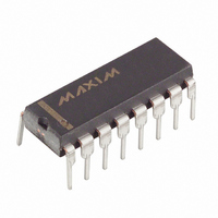
DS232A-N Maxim Integrated Products, DS232A-N Datasheet

DS232A-N
Specifications of DS232A-N
Related parts for DS232A-N
DS232A-N Summary of contents
Page 1
... Meets all EIA-232E and V.28 specifications Uses small capacitors: 0.1 μF Optional industrial temperature range available (-40°C to +85°C) ORDERING INFORMATION DS232A 16-pin DIP DS232A-N 16-pin DIP (Industrial) DS232AR 16-pin SOIC (150-Mil) DS232AR-N 16-pin SOIC (150-Mil) (Industrial) DS232AS 16-pin SOIC (300-Mil) ...
Page 2
... FUNCTIONAL DIAGRAM OF DS232A Figure 1 NOTE recommended decoupling capacitor which is the same value as C1, C2, C3, and C4 Are for TSSOP package only. PIN DESCRIPTIONS V , GND: DC power is provided to the device on these pins V+: Positive supply output (RS-232). V+ requires an external storage charge capacitor of at least 0.1 μF. ...
Page 3
... V+. Likewise, C2 can be omitted if -12V is connected directly to V-. DUAL CHARGE PUMP CONVERTERS The DS232A has a two-stage on-board charge pump circuit that is used to generate ±10 volts from a single +5-volt supply. In the first stage, capacitor C1 doubles the +5V supply to +10 volts which is then stored on capacitor C3. The second stage uses capacitor C2 to invert the +10V potential to -10V. This charge is then stored on capacitor C4. The ± ...
Page 4
... SYMBOL MIN TYP I 4 CC1 I 15 CC2 ±5 ±8 V ORS V 0.8 1.4 TTL V 1.4 TTH f 250 350 300 10M OUT ±15 ±30 I TSC DS232A (0°C to 70°C) MAX UNITS NOTES 5 (0°C to 70°C) MAX UNITS NOTES 2 bits/s μA 40 Ω 3 ±100 mA 4 ...
Page 5
... PLHR t PHLT -t PLHT t PHLR -t PLHR = ±2V 25° (0°C to 70°C) ±30 V 1.3 V 1.8 2 kΩ 0 (0°C to 70°C) TYP MAX UNITS NOTES 12 30 V/μs μs 1.3 3.5 μs 1.5 3.5 μs 0.5 1 μs 0.6 1 300 ns 100 ns DS232A ...
Page 6
... TRANSMITTER PROPAGAION DELAY TIMING Figure 2 RECEIVER PROPAGATION DELAY TIMING Figure DS232A ...
Page 7
... C IN. 0.120 0.140 MM 3.05 3.56 D IN. 0.300 0.325 MM 7.62 8.26 E IN. 0.015 0.040 MM 0.38 1.02 F IN. 0.120 0.140 MM 3.04 3.56 G IN. 0.090 0.110 MM 2.29 2.79 H IN. 0.320 0.370 MM 8.13 9.40 J IN. 0.008 0.012 MM 0.20 0.30 K IN. 0.015 0.021 MM 0.38 0. DS232A ...
Page 8
... B IN. 0.012 0.020 MM 0.30 0.50 C IN. 0.007 0.011 MM 0.17 0.28 D IN. 0.386 0.393 MM 9.80 9.98 E IN. 0.050 BSC MM 1.27 BSC E1 IN. 0.150 0.158 MM 3.81 4.01 H IN. 0.230 0.244 MM 5.84 6.20 L IN. 0.016 0.050 MM 0.40 0.89 Θ 0° 8° DS232A ...
Page 9
... IN. 0.013 0.020 0.51 MM 0.33 C IN. 0.009 0.013 MM 0.229 0.33 D IN. 0.398 0.412 MM 10.11 10.46 E IN. 0.050 BSC MM 1.27 BSC E1 IN. 0.290 0.300 MM 7.37 7.62 H IN. 0.398 0.416 MM 10.11 10.57 L IN. 0.016 0.040 MM 0.40 1.02 Θ 0° 8° DS232A ...
Page 10
... TSSOP DIM MIN MAX 1. 0. 0.75 1. 0.09 0. 0.50 0. 0.65 BSC B MM 0.18 0. 6.40 6. 4.40 NOM G MM 0.25 REF H MM 6.25 6.55 phi 0° 8° DS232A ...


