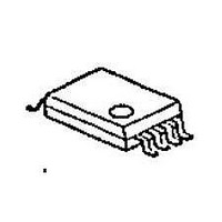
NJM2115V-TE1 NJR, NJM2115V-TE1 Datasheet - Page 2

NJM2115V-TE1
Manufacturer Part Number
NJM2115V-TE1
Description
Op Amps Dual
Manufacturer
NJR
Datasheet
1.NJM2115V-TE1.pdf
(5 pages)
Specifications of NJM2115V-TE1
Number Of Channels
2
Voltage Gain Db
80 dB
Common Mode Rejection Ratio (min)
60 dB
Input Offset Voltage
6 mV
Supply Current
5 mA
Maximum Power Dissipation
800 mW
Maximum Operating Temperature
+ 85 C
Mounting Style
SMD/SMT
Package / Case
SSOP-8
Maximum Dual Supply Voltage
+/- 7 V
Minimum Operating Temperature
- 40 C
Lead Free Status / Rohs Status
Details
Available stocks
Company
Part Number
Manufacturer
Quantity
Price
Company:
Part Number:
NJM2115V-TE1
Manufacturer:
NJR
Quantity:
1 833
■ ABSOLUTE MAXIMUM RATINGS
Supply Voltage
Differential Input Voltage
Power Dissipation
Operating Temperature Range
Storage Temperature Range
■ ELECTRICAL CHARACTERISTICS
Input Offset Voltage
Input Bias Current
Large Signal Voltage Gain
Maximum Output Voltage Swing
Input Common Mode Voltage Range
Common Mode Rejection Ratio
Supply Voltage Rejection Ratio
Operating Current
Slew Rate
Gain Bandwidth product
( Note1 ) Applied circuit voltage gain is desired to be operated within the range of 3dB to 30 dB.
( Note2 ) Special care being required for input common mode voltage range and the oscillation due to the capacitive load when operating on voltage follower.
- 2 -
PARAMETER
PARAMETER
SYMBOL
SYMBOL
CMR
V
SVR
V
V
T
T
SR
GB
V
V
P
A
I
+
I
CC
ICM
opr
OM
stg
B
/V
ID
IO
D
V
-
f=10kHz
R
R
R
V
A
S
L
L
IN
V
≥10kΩ
≥2.5kΩ
=1,V
≤
=0,R
10kΩ
TEST CONDITION
IN
L
( SSOP8 ) 250
=∞
=± 1V
( DMP8 ) 300
( DIP8 ) 500
( SIP8 ) 800
RATINGS
-40~+125
-40~+85
± 7.0
± 14
( Ta=25˚C )
UNIT
± 1.5
MIN.
mW
± 2
˚C
˚C
60
60
60
V
V
-
-
-
-
-
( V
TYP.
± 2.2
100
3.5
80
74
80
12
1
4
-
+
/V
-
=±2.5V
Ver.2003-03-17
MAX.
300
,
6
5
-
-
-
-
-
-
-
Ta=25˚C )
UNIT
V/µs
MHz
mV
mA
nA
dB
dB
dB
V
V


