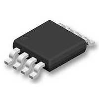
LM4961LQ National Semiconductor, LM4961LQ Datasheet

LM4961LQ
Specifications of LM4961LQ
Available stocks
Related parts for LM4961LQ
LM4961LQ Summary of contents
Page 1
... External gain configuration capability ■ Including Band exchange SW ■ Including Leakage cut SW Applications ■ Cellphone ■ PDA LM4961LQ (5x5) Top View Order Number LM4961LQ See NS Package Number LQA28A 200940 December 2006 7mA (typ) 15Vp-p (typ) 0.1μA (typ) = 2μF+30Ω 1kHz L 20094084 www.national.com ...
Page 2
Typical Application * R is needed for over/under voltage protection. If inputs are less than V C when in shutdown mode, then R can be shorted 1.23V FB Receiver Mode (BW2) Ringer Mode (BW1) Shutdown www.national.com ...
Page 3
... Absolute Maximum Ratings If Military/Aerospace specified devices are required, please contact the National Semiconductor Sales Office/ Distributors for availability and specifications. Supply Voltage ( Amplifier Supply Voltage ( Storage Temperature Input Voltage Power Dissipation (Note 3) ESD Susceptibility (Note 4) ESD Susceptibility (Note 5) Electrical Characteristics V The following specifications apply for V specified. Limits apply for T = 25° ...
Page 4
Electrical Characteristics V The following specifications apply for V specified. Limits apply for T = 25°C. A Symbol Parameter I Quiescent Power Supply Current DD Iddrcv Iq in receiver mode I Shutdown Current SD V Logic High Threshold Voltage LH ...
Page 5
Typical Performance Characteristics THD+N vs Frequency V = 4.2V 14V , P-P THD+N vs Output Voltage = 2μF + 30Ω 4.2V PSRR vs Frequency = 8Ω 4.2V, ...
Page 6
Power Dissipation vs Output Power = 2μF + 30Ω 1kHz V = 4.2V Supply Current vs Supply Voltage = 2μF + 30Ω 0V Switch Current Limit vs Duty Cycle ...
Page 7
Feedback Voltage vs Temperature 20094097 Max. Duty Cycle vs Temperature - ”X” 200940a0 R (ON 200940a2 Feedback Bias Current vs Temperature R (ON Temperature 7 20094098 200940a1 www.national.com ...
Page 8
... This plane forms a thermal mass, heat sink, and radiation area. Further detailed and specific information concerning PCB layout, fabrication, and mounting an LD (LLP) package is found in National Semiconductor’s Package Engineering Group under application note AN1187. SHUTDOWN FUNCTION In many applications, a microcontroller or microprocessor output is used to control the shutdown circuitry to provide a quick, smooth transition into shutdown ...
Page 9
Band-SW pin (pin 19) the amplifier ringer mode. This enables the boost converter and sets the externally configurable closed loop gain selection to BW1. If the Band-SW pin has a logic ...
Page 10
POWER SUPPLY BYPASSING As with any amplifier, proper supply bypassing is critical for low noise performance and high power supply rejection. The capacitor location on both V1 and the device as possible. SELECTING INPUT CAPACITOR FOR AUDIO ...
Page 11
DUTY CYCLE The maximum duty cycle of the boost converter determines the maximum boost ratio of output-to-input voltage that the converter can attain in continuous mode of operation. The duty cycle for a given boost application is defined as: Duty ...
Page 12
Resis- tance" of the FET times the average inductor current. FET on resistance increases the internal N-FET has less gate voltage in this input voltage range (see Typical Performance ...
Page 13
Schematic Board Layout FIGURE 4. Demo Board Schematic 13 200940a4 www.national.com ...
Page 14
Demonstration Board Layout www.national.com FIGURE 5. Recommended TS SE PCB Layout: Top Silkscreen FIGURE 6. Recommended TS SE PCB Layout: Top Layer 14 200940c1 200940c0 ...
Page 15
FIGURE 7. Recommended TS SE PCB Layout: Bottom Layer 15 200940c2 www.national.com ...
Page 16
Revision History Rev Date 1.0 08/25/04 1.1 11/14/05 1.2 08/30/06 Added the TWUA row in the 4.2V Elect. Char table, then released the D/S to the WEB. 1.3 09/11/06 Added the “Selecting Value For Rc” in the Apps section, then ...
Page 17
... Physical Dimensions inches (millimeters) unless otherwise noted LQ Package Order Number LM4961LQ NS Package Number LQA28A 17 www.national.com ...
Page 18
... National Semiconductor and the National Semiconductor logo are registered trademarks of National Semiconductor Corporation. All other brand or product names may be trademarks or registered trademarks of their respective holders. ...


