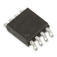
LTC6102IMS#PBF Linear Technology, LTC6102IMS#PBF Datasheet - Page 20

LTC6102IMS#PBF
Manufacturer Part Number
LTC6102IMS#PBF
Description
AMP, CURRENT SENSE, PRECISION, SMD
Manufacturer
Linear Technology
Datasheet
1.LTC6102CDDPBF.pdf
(26 pages)
Specifications of LTC6102IMS#PBF
No. Of Amplifiers
1
Input Bias Current
3nA
Output Current Per Channel
1mA
Input Offset Voltage
5µV
Bandwidth
200kHz
Supply Voltage Range
4V To 60V
Supply Current
650µA
Rohs Compliant
Yes
Available stocks
Company
Part Number
Manufacturer
Quantity
Price
LTC6102
LTC6102-1/LTC6102HV
pin. Figure 11 shows the LTC6102-1 with a 2.7M pull-up
resistor to limit the current to less than 20μA with a 60V
supply, which is enough to satisfy the input bias current
requirement.
Start-Up Current
The start-up current of the LTC6102 when the part is
powered on or enabled (LTC6102-1) consists of three
parts: the fi rst is the current necessary to charge the
V
V
voltage, this can require a signifi cant amount of start-up
current. The second source is the active supply current of
the LTC6102 amplifi er, which is not signifi cantly greater
during start-up than during normal operation. The third
source is the output current of the LTC6102, which upon
start-up may temporarily drive the output high. This could
cause milliamps of output current (limited mostly by the
APPLICATIONS INFORMATION
20
REG
REG
R
SENSE
bypass capacitor, which is nominally 0.1μF . Since the
voltage charges to approximately 4.5V below the V
R
2.7M
LOAD
BIAS
V
+
R
R
IN
IN
–
+
+IN
V
EN
–
R
IN
LTC6102-1
+
=
R
+
IN
Figure 11
–
–
R
SENSE
–
–INS
V
OUT
–INF
V
REG
+
6102 F11
R
OUT
V
OUT
0.1μF
+
input resistor R
the output limiting ESD structure in the LTC6102. This is
a temporary condition which will cease when the LTC6102
amplifi er settles into normal closed-loop operation.
When the LTC6102-1 is disabled, the internal amplifi er is
also shut down, which means that the discharge rate of
the 0.1μF capacitor is very low. This is signifi cant when the
LTC6102-1 is disabled to save power, because the recharg-
ing of the 0.1μF capacitor is a signifi cant portion of the
overall power consumed in startup. Figure 12 shows the
discharge rate of the 0.1μF capacitor after the LTC6102-1
is shut down at room temperature.
In a system where the LTC6102-1 is disabled for short
periods, the start-up power (and therefore the average
power) can be reduced since the V
is never signifi cantly discharged. The time required to
charge the V
the LTC6102-1 to start-up more quickly.
2.25
2.00
1.75
1.50
1.25
1.00
0.75
0.50
0.25
Figure 12. LTC6102-1 V
Bypass Capacitor Discharge when Disabled
0
REG
–2
IN
0
capacitor will also be reduced, allowing
) to fl ow into the output resistor and/or
2
4
TIME (ms)
6
8
REG
10
Voltage During
V
EN
REG
REG
12
T
V
A
+
= 25°C
= 12V
14
bypass capacitor
6102 F12
16
8.3
8.2
8.1
8.0
7.9
7.8
7.7
7.6
7.5
7.4
6102fd


