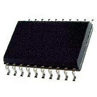
MC100EL17DW ON Semiconductor, MC100EL17DW Datasheet - Page 4

MC100EL17DW
Manufacturer Part Number
MC100EL17DW
Description
Buffers & Line Drivers 5V ECL Quad Diff
Manufacturer
ON Semiconductor
Datasheet
1.MC100EL17DW.pdf
(6 pages)
Specifications of MC100EL17DW
Logic Family
100EL
Logic Type
Quad Differential Receiver
Supply Voltage (max)
- 5.7 V, 5.7 V
Supply Voltage (min)
- 4.2 V, 4.2 V
Maximum Operating Temperature
+ 85 C
Mounting Style
SMD/SMT
Package / Case
SO-20 WB
Minimum Operating Temperature
- 40 C
Number Of Lines (input / Output)
/ /
Supply Current
33 mA
Lead Free Status / Rohs Status
No RoHS Version Available
Available stocks
Company
Part Number
Manufacturer
Quantity
Price
Company:
Part Number:
MC100EL17DWG
Manufacturer:
ON Semiconductor
Quantity:
135
Company:
Part Number:
MC100EL17DWR2
Manufacturer:
ON
Quantity:
8 450
Part Number:
MC100EL17DWR2
Manufacturer:
MOTOROLA/摩托罗拉
Quantity:
20 000
Table 6. AC CHARACTERISTICS
NOTE: Device will meet the specifications after thermal equilibrium has been established when mounted in a test socket or printed circuit
8. V
9. Skews are valid across specified voltage range, part−to−part skew is for a given temperature.
10. Duty cycle skew is the difference between a t
11. V
f
t
t
t
t
V
t
t
Symbol
MAX
PLH
PHL
SKEW
JITTER
r
f
PP
EE
PP
(min) is minimum input swing for which AC parameters guaranteed. The device has a DC gain of ≈ 40.
board with maintained transverse airflow greater than 500 lfpm. Electrical parameters are guaranteed only over the declared
operating temperature range. Functional operation of the device exceeding these conditions is not implied. Device specification limit
values are applied individually under normal operating conditions and not valid simultaneously.
can vary +0.8 V / −0.5 V.
Maximum Toggle Frequency
Propagation Delay
D to Q
Skew
Random Clock Jitter (RMS)
Input Swing (Note 11)
Output Rise/Fall Times Q
(20% − 80%)
Part−to−Part (Diff) (Note 9)
Output−to−Output (Note 9)
Duty Cycle (Diff) (Note 10)
Characteristic
(See Application Note AND8020/D − Termination of ECL Logic Devices.)
Figure 2. Typical Termination for Output Driver and Device Evaluation
Driver
Device
Single−Ended
V
Differential
CC
Q
Q
= 5.0 V; V
PLH
and t
EE
Min
330
280
150
280
= 0 V or V
PHL
Z
Z
http://onsemi.com
o
o
= 50 W
= 50 W
propagation delay through a device.
−40°C
Typ
CC
50 W
V
4
TT
= 0 V; V
= V
1000
Max
530
580
200
550
75
25
V
CC
TT
EE
− 3.0 V
50 W
Min
350
300
150
280
= −5.0 V (Note 8)
25°C
1.75
Typ
0.7
D
D
1000
Max
550
600
200
550
75
25
Receiver
Device
Min
360
310
150
280
85°C
Typ
1000
Max
560
610
200
550
75
25
GHz
Unit
mV
ps
ps
ps
ps


