NLSF3T125MNR2 ON Semiconductor, NLSF3T125MNR2 Datasheet - Page 2
NLSF3T125MNR2
Manufacturer Part Number
NLSF3T125MNR2
Description
Buffers & Line Drivers 2-5.5V Quad Bus
Manufacturer
ON Semiconductor
Datasheet
1.NLSF3T125MNR2.pdf
(8 pages)
Specifications of NLSF3T125MNR2
Logic Family
NLSF
Logic Type
CMOS
Number Of Channels Per Chip
4
Polarity
Non-Inverting
Supply Voltage (max)
5.5 V
Supply Voltage (min)
2 V
Maximum Operating Temperature
+ 85 C
Mounting Style
SMD/SMT
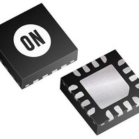
Package / Case
QFN-16
High Level Output Current
- 8 mA
Low Level Output Current
8 mA
Maximum Power Dissipation
500 mW
Minimum Operating Temperature
- 40 C
Number Of Lines (input / Output)
4 / 3
Output Type
3-State
Propagation Delay Time
11.5 ns at 3.3 V
Lead Free Status / Rohs Status
No RoHS Version Available
Available stocks
Company
Part Number
Manufacturer
Quantity
Price
Company:

Part Number:
NLSF3T125MNR2
Manufacturer:
MIC
Quantity:
200
Company:
Part Number:
NLSF3T125MNR2G
Manufacturer:
SWITCHCOR
Quantity:
108


Î Î Î Î Î Î Î Î Î Î Î Î Î Î Î Î Î Î Î Î Î Î Î
Î Î Î Î Î Î Î Î Î Î Î Î Î Î Î Î Î Î Î Î Î Î Î
Î Î Î Î
Î Î Î Î
Î Î Î Î
Î Î Î Î
Î Î Î Î
Î Î Î Î
Î Î Î Î
Î Î Î Î
Î Î Î Î
Î Î Î Î
Î Î Î Î
Î Î Î Î
Î Î Î Î
Î Î Î Î
Î Î Î Î
Î Î Î Î
Î Î Î Î
Î Î Î Î
Î Î Î Î
Î Î Î Î
Î Î Î Î
Î Î Î Î
Î Î Î Î
Î Î Î Î
Î Î Î Î
Î Î Î Î
Î Î Î Î
Î Î Î Î
Î Î Î Î
Î Î Î Î
Î Î Î Î
Î Î Î Î
Î Î Î Î
Î Î Î Î
Maximum ratings applied to the device are individual stress limit values (not normal operating conditions) and are not valid simultaneously. If
stress limits are exceeded device functional operation is not implied, damage may occur and reliability may be affected. Functional operation
should be restricted to the Recommended Operating Conditions.
MAXIMUM RATINGS
RECOMMENDED OPERATING CONDITIONS
Symbol
Symbol
V
V
T
I
I
V
I
P
V
V
I
OK
out
CC
t
V
stg
CC
out
IK
T
r
in
, t
D
CC
out
in
A
f
Î Î Î Î Î Î Î Î Î Î Î Î Î Î Î Î Î Î Î Î Î Î Î Î Î
Î Î Î Î Î Î Î Î Î Î Î Î Î Î
Î Î Î Î Î Î Î Î Î Î Î Î Î Î
Î Î Î Î Î Î Î Î Î Î Î Î Î Î
Î Î Î Î Î Î Î Î Î Î Î Î Î Î
Î Î Î Î Î Î Î Î Î Î Î Î Î Î
Î Î Î Î Î Î Î Î Î Î Î Î Î Î
Î Î Î Î Î Î Î Î Î Î Î Î Î Î
Î Î Î Î Î Î Î Î Î Î Î Î Î Î
Î Î Î Î Î Î Î Î Î Î Î Î Î Î
Î Î Î Î Î Î Î Î Î Î Î Î Î Î
Î Î Î Î Î Î Î Î Î Î Î Î Î Î
Î Î Î Î Î Î Î Î Î Î Î Î Î Î
Î Î Î Î Î Î Î Î Î Î Î Î Î Î
Î Î Î Î Î Î Î Î Î Î Î Î Î Î
Î Î Î Î Î Î Î Î Î Î Î Î Î Î
Î Î Î Î Î Î Î Î Î Î Î Î Î Î
Î Î Î Î Î Î Î Î Î Î Î Î Î Î
Î Î Î Î Î Î Î Î Î Î Î Î Î Î
Î Î Î Î Î Î Î Î Î Î Î Î Î Î
Î Î Î Î Î Î Î Î Î Î Î Î Î Î
Î Î Î Î Î Î Î Î Î Î Î Î Î Î
Î Î Î Î Î Î Î Î Î Î Î Î Î Î Î Î Î Î Î Î Î Î Î Î Î
Î Î Î Î Î Î Î Î Î Î Î Î Î Î Î Î Î Î Î Î Î Î Î Î Î
Î Î Î Î Î Î Î Î Î Î Î Î Î Î Î Î Î Î Î Î Î Î Î Î Î
Î Î Î Î Î Î Î Î Î Î Î Î Î Î Î Î Î Î Î Î Î Î Î Î Î
Î Î Î Î Î Î Î Î Î Î Î Î Î Î Î Î Î Î Î Î Î Î Î Î Î
Î Î Î Î Î Î Î Î Î Î Î Î Î Î Î Î Î Î Î Î Î Î Î Î Î
Î Î Î Î Î Î Î Î Î Î Î Î Î Î Î Î Î Î Î Î Î Î Î Î Î
Î Î Î Î Î Î Î Î Î Î Î Î Î Î Î Î Î Î Î Î Î Î Î Î Î
Î Î Î Î Î Î Î Î Î Î Î Î Î Î Î Î Î Î Î Î Î Î Î Î Î
Î Î Î Î Î Î Î Î Î Î Î Î Î Î Î Î Î Î Î Î Î Î Î Î Î
Î Î Î Î Î Î Î Î Î Î Î Î Î Î Î Î Î Î Î Î Î Î Î Î Î
Î Î Î Î Î Î Î Î Î Î Î Î Î Î Î Î Î Î Î Î Î Î Î Î Î
DC Supply Voltage
DC Input Voltage
DC Output Voltage
Input Diode Current
Output Diode Current (V
DC Output Current, per Pin
DC Supply Current, V
Power Dissipation in Still Air,
Storage Temperature
DC Supply Voltage
DC Input Voltage
DC Output Voltage
Operating Temperature
Input Rise and Fall Time
Parameter
CC
OUT
and GND Pins
< GND; V
OE2
NC
Y1
A2
High or Low State
Figure 2. QFN − 16 Pinout (Top View)
Output in 3−State
QFN Packages
OUT
1
2
3
4
V
CC
High or Low State
Output in 3−State
> V
= 5.0 V
Parameter
A1
Y2
CC
16
http://onsemi.com
5
)
NLSF3T125
GND Y3
OE1 V
15
6
Î Î Î Î Î
Î Î Î Î Î
Î Î Î Î Î
Î Î Î Î Î
Î Î Î Î Î
Î Î Î Î Î
Î Î Î Î Î
Î Î Î Î Î
Î Î Î Î Î
Î Î Î Î Î
Î Î Î Î Î
Î Î Î Î Î
Î Î Î Î Î
Î Î Î Î Î
Î Î Î Î Î
Î Î Î Î Î
Î Î Î Î Î
Î Î Î Î Î
Î Î Î Î Î
Î Î Î Î Î
Î Î Î Î Î
0.5 V
– 0.5 to V
2
– 0.5 to + 7.0
– 0.5 to + 7.0
– 0.5 to + 7.0
– 65 to + 150
CC
14
7
Value
− 20
500
20
25
75
OE4
CC
13
A3
8
+ 0.5
Î Î Î
Î Î Î
Î Î Î
Î Î Î
Î Î Î
Î Î Î
Î Î Î
Î Î Î
Î Î Î
Î Î Î
Î Î Î
Î Î Î
Î Î Î
Î Î Î
Î Î Î
Î Î Î
Î Î Î
Î Î Î
Î Î Î
Î Î Î
Î Î Î
12
11
10
9
Unit
mW
mA
mA
mA
mA
V
V
V
A4
NC
Y4
OE3
C
Exposed Pad (EP)
circuitry to guard against damage
due to high static voltages or electric
fields. However, precautions must
be taken to avoid applications of any
voltage higher than maximum rated
voltages to this high−impedance cir-
cuit. For proper operation, V
V
range GND v (V
tied to an appropriate logic voltage
level (e.g., either GND or V
Unused outputs must be left open.
out
This device contains protection
Unused inputs must always be
should be constrained to the
Î Î Î
Î Î Î
Î Î Î
Î Î Î
Î Î Î
Î Î Î
Î Î Î
Î Î Î
Î Î Î
Î Î Î
Î Î Î
Î Î Î
Î Î Î
− 40
Min
2.0
0
0
0
0
in
Î Î Î
Î Î Î
Î Î Î
Î Î Î
Î Î Î
Î Î Î
Î Î Î
Î Î Î
Î Î Î
Î Î Î
Î Î Î
Î Î Î
Î Î Î
or V
+ 85
Max
V
5.5
5.5
5.5
20
CC
out
) v V
Î Î Î Î
Î Î Î Î
Î Î
Î Î
Î Î
Î Î
Î Î
Î Î
Î Î
Î Î
Î Î
Unit
ns/V
in
V
V
V
C
CC
CC
and
).
.
Related parts for NLSF3T125MNR2
Image
Part Number
Description
Manufacturer
Datasheet
Request
R

Part Number:
Description:
Quad Bus Buffer
Manufacturer:
ONSEMI [ON Semiconductor]
Datasheet:

Part Number:
Description:
ON Semiconductor [VOLTAGE REGULATOR]
Manufacturer:
ON Semiconductor
Datasheet:
Part Number:
Description:
357-036-542-201 CARDEDGE 36POS DL .156 BLK LOPRO
Manufacturer:
ON Semiconductor
Datasheet:
Part Number:
Description:
357-036-542-201 CARDEDGE 36POS DL .156 BLK LOPRO
Manufacturer:
ON Semiconductor
Datasheet:
Part Number:
Description:
357-036-542-201 CARDEDGE 36POS DL .156 BLK LOPRO
Manufacturer:
ON Semiconductor
Datasheet:
Part Number:
Description:
357-036-542-201 CARDEDGE 36POS DL .156 BLK LOPRO
Manufacturer:
ON Semiconductor
Datasheet:
Part Number:
Description:
357-036-542-201 CARDEDGE 36POS DL .156 BLK LOPRO
Manufacturer:
ON Semiconductor
Datasheet:
Part Number:
Description:
357-036-542-201 CARDEDGE 36POS DL .156 BLK LOPRO
Manufacturer:
ON Semiconductor
Datasheet:
Part Number:
Description:
357-036-542-201 CARDEDGE 36POS DL .156 BLK LOPRO
Manufacturer:
ON Semiconductor
Datasheet:
Part Number:
Description:
357-036-542-201 CARDEDGE 36POS DL .156 BLK LOPRO
Manufacturer:
ON Semiconductor
Datasheet:
Part Number:
Description:
357-036-542-201 CARDEDGE 36POS DL .156 BLK LOPRO
Manufacturer:
ON Semiconductor
Datasheet:
Part Number:
Description:
357-036-542-201 CARDEDGE 36POS DL .156 BLK LOPRO
Manufacturer:
ON Semiconductor
Datasheet:
Part Number:
Description:
Manufacturer:
ON Semiconductor
Datasheet:
Part Number:
Description:
Manufacturer:
ON Semiconductor
Datasheet: