CS4954-CQZ Cirrus Logic Inc, CS4954-CQZ Datasheet
CS4954-CQZ
Specifications of CS4954-CQZ
Available stocks


Related parts for CS4954-CQZ


CS4954-CQZ Summary of contents
Page 1
... Parallel or high-speed I²C compatible control interfaces are provided for flexibility in system design. The parallel interface doubles as a general purpose I/O port when the CS4954 I²C mode to help conserve valuable board area. The CS4954 and CS4955 are available in a 48-pin TQFP and operate in -40 to +85° ...
Page 2
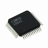
... ORDERING INFORMATION Product Description CS4954 NTSC/PAL Digital Video Encoder CS4955 CDB4954/55 CS4954/55 Evaluation Board 2 Package Pb-Free Grade 48-TQFP Yes Commercial -40º to +85º CS4954 CS4955 Temp Range Container Order# CS4954-CQZ Rail CS4955-CQZ - - CDB4954A/55A DS278F6 ...
Page 3
... TABLE OF CONTENTS 1. CHARACTERISTICS AND SPECIFICATIONS ........................................................................................6 AC & DC PARAMETRIC SPECIFICATIONS ............................................................................................6 RECOMMENDED Operating Conditions .......................................................................................................6 THERMAL CHARACTERISTICS ..............................................................................................................6 DC CHARACTERISTICS ..........................................................................................................................6 AC CHARACTERISTICS ..........................................................................................................................8 TIMING CHARACTERISTICS ...................................................................................................................9 2. ADDITIONAL CS4954/5 FEATURES .....................................................................................................11 3. CS4954 INTRODUCTION ......................................................................................................................11 4. FUNCTIONAL DESCRIPTION ...............................................................................................................11 4.1 Video Timing Generator ...............................................................................................................11 4.2 Video Input Formatter ..................................................................................................................12 4.3 Color Subcarrier Synthesizer .......................................................................................................12 4 ...
Page 4
... BOARD DESIGN AND LAYOUT CONSIDERATIONS ......................................................................... 53 9.1 Power and Ground Planes .......................................................................................................... 53 9.2 Power Supply Decoupling ........................................................................................................... 53 9.3 Digital Interconnect ...................................................................................................................... 53 9.4 Analog Interconnect ..................................................................................................................... 53 9.5 Analog Output Protection ............................................................................................................ 54 9.6 ESD Protection ............................................................................................................................ 54 9.7 External DAC Output Filter .......................................................................................................... 54 10. PIN DESCRIPTION ............................................................................................................................... 56 11. PACKAGE DRAWING ........................................................................................................................... 58 12. REVISION HISTORY ............................................................................................................................. 59 4 CS4954 CS4955 DS278F6 ...
Page 5
... I²C Protocol.............................................................................................................35 Figure 27. 8-bit Parallel Host Port Timing: Read-Write/Write-Read Cycle...............................35 Figure 28. 8-bit Parallel Host Port Timing: Address Read Cycle .............................................36 Figure 29. 8-bit Parallel Host Port Timing: Address Write Cycle .............................................36 Figure 30. External Low Pass Filter .........................................................................................54 Figure 31. Typical Connection Diagram...................................................................................55 5 CS4954 CS4955 DS278F6 ...
Page 6
... Symbol VAA/VDD Symbol θ (Four-layer PCB) TQFP JA-TM θ (Two-layer PCB) TQFP JA- 25° C; VAA, VDD = 5 V; GNDA, GNDD = 0 V.) A Symbol VIH VIH VOH VOL CS4954 CS4955 Min Max -0.3 6.0 -10 10 -50 +50 -0.3 VAA + 0.3 -0.3 VDD + 0.3 -55 + 125 -65 + 150 ...
Page 7
... UVC VAA, VDD IAA1 Low-Z (Note 6) IAA2 High-Z (Note 7) IAA3 PSRR (Note 1) (Note 1) DNL (Note 1) INL (Note 1) DG (Note 1) DP (Note 1) HA SNR (Note 1) SAT CS4954 CS4955 Min Typ Max - - 0.4 - -10 - +10 IO 32.9 34.7 36.5 IO 8.22 8.68 9.13 IB 32.2 33.9 35 ...
Page 8
... Clock to Data Hold Time Clock to Data Output Delay CLK T ch V[7:0] HSYNC/VSYNC (Inputs) HSYNC/VSYNC (1) CB/FIELD /INT (Outputs isu Figure 1. Video Pixel Data and Control Port Timing CS4954 CS4955 Symbol Min Typ Max Tch 14.82 18.52 22.58 Tcl 14.82 18.52 22.58 Tisu Tih ...
Page 9
... SCL Low to Data Out Valid SDA SCL DS278F6 sph vdo T T spi si Figure 2. I²C Host Port Timing CS4954 CS4955 Symbol Min Typ Max Fclk 1000 Tsph 0.1 Tspl 0.7 Tsh 100 Tssu 100 Tsds 50 Tsr 1 Tsf 0.3 Tss 100 Tbuf ...
Page 10
... Write Data Hold Time Write-Read/Read-Write Recovery Time Address from Write Hold Time Reset Timing (Figure 3) Reset Pulse Width RESET* 10 (Continued) Symbol Trd Trpw Tas Trah Trda Trdh Twr Twpw Twds Twdh Trec Twac Tres T res Figure 3. Reset Timing CS4954 CS4955 Min Typ Max Units ...
Page 11
... The CS4954/5 is completely configured and con- trolled via an 8-bit host interface port or an I²C compatible serial interface. This host port provides access and control of all CS4954/5 options and fea- tures, such as closed caption insertion, interrupts, etc. In order to lower overall system costs, the ...
Page 12
... In both Master and Slave Modes, all timing is sampled and assert- ed with the rising edge of the CLK pin. In most cases, the CS4954/5 will serve as the video timing master. HSYNC, VSYNC, and FIELD are configured as outputs in Master Mode. HSYNC or FIELD can also be defined as a composite blank- ing output signal in Master Mode ...
Page 13
... Luma Path Along with the chroma output path, the CS4954/5 Video Input Formatter has a parallel luma data out- put to a digital delay line. The delay line is a digital FIFO. The FIFO depth matches the clock period delay associated with the more complex chroma path ...
Page 14
... Host Interface The CS4954/5 provides a parallel 8-bit data inter- face for overall configuration and control. The host interface uses active-low read and write strobes, along with an active-low address enable signal, to provide microprocessor-compatible read and write cycles ...
Page 15
... While the RESET pin is held low, the host interface in the CS4954/5 is disabled and will not respond to host-initiated bus cycles. All outputs are valid after a time period following RESET pin low. A device RESET initializes the CS4954/5 internal registers to their default values as described by Ta- ble 9, Control Registers ...
Page 16
... Mode, the Sync Generator uses externally provided horizontal and vertical sync signals to synchronize the internal timing of the CS4954/5. Video data that is sent to the CS4954/5 must be synchronized to the horizontal and vertical sync signals. Figure trates horizontal timing for ITU R.BT601 input in Slave Mode. Note that the CS4954/5 expects to re- ...
Page 17
... Active Lines 285 through line 525. 22-261; 285-524 5.2.6 PAL Interlaced 23-310; The CS4954/5 supports PAL modes 336-623 22-261 N, and Combination N, in which there are 625 total 23-310 lines per frame, two fixed 312.5 line fields per frame, and 25 total frames per second. Figure lustrates PAL interlaced vertical timing ...
Page 18
... NTSC interlaced tim- ing is illustrated in Figure 9. In this mode, the CS4954/5 expects digital video input at the V [7:0] pins for 240 lines beginning on active video line 22 and continuing through line 261. ...
Page 19
... PAL non-interlaced tim- ing is illustrated in Figure 10. In this mode, the CS4954/5 expects digital video input on the V [7:0] pins for 288 lines, beginning on active video line 23 and continuing through line 309. ...
Page 20
... Burst Phase = 225 degrees relative to U Figure 8. PAL Video Interlaced Timing setting the 656_SYNC_OUT register bit in CONTROL_6 register, HSYNC and VSYNC are output,so that other devices in the system can syn- chronize to these timing signals. CS4954 CS4955 318 319 320 ...
Page 21
... Burst phase = reference phase = 180 relative to B-Y 5.5 Multi-standard Output Format Modes The CS4954/5 supports a wide range of output for- mats compatible with worldwide broadcast stan- dards. These formats include NTSC-M, NTSC-J, PAL-B/D/G/H/I, PAL-M, PAL-N, and PAL Com- bination N (PAL-Nc) which is the broadcast stan- dard used in Argentina ...
Page 22
... V[7:0] Cr DATA EAV Code 4 Clocks Active Video 5.6 Subcarrier Generation The CS4954/5 automatically synthesizes NTSC and PAL color subcarrier clocks using the CLK fre- quency and four control (SC_SYNTH0/1/2/3). The NTSC subcarrier syn- thesizer is reset every four fields (every eight fields for PAL) ...
Page 23
... MPEG-2 system clock. Sub-carrier compensation is enabled through the XTAL bit of the CONTROL_2 Register. When enabled, the 43ED288D CS4954/5 will utilize a common quartz color burst 43CDDFC7 crystal (3.579545 MHz ± 50 ppm for NTSC) at- tached to the XTAL_IN and XTAL_OUT pins to automatically compare and compensate the color subcarrier synthesis process ...
Page 24
... TTXRQ output signal a sin- gle teletext bit has to be provided after a program- mable input delay at the TTXDAT input pin. Phase variant interpolation of the data in the inter- nal teletext encoder results in minimal phase jitter on the ouput text lines. CS4954 CS4955 DS278F6 ...
Page 25
... MHz clock. The pulse width of the TTXRQ signal varies between three and four 27 MHz clock cycles. The variation is necessary in CVBS/Y t TTXWin TTXRQ TTXDAT Figure 13. Teletext Timing (Window Mode) CS4954 CS4955 is the internally used insertion TTXWin TTX_LINE_DIS2 t t TTXWin TTX textbit #: ...
Page 26
... PAL-N (Arg.) Table 5. Teletext timing parameters 5.12 Color Bar Generator The CS4954/5 is equipped with a color bar genera- tor that is enabled through the CBAR bit of the CONTROL_1 Register. The color bar generator works in Master or Slave Mode and has no effect on the video input/output timing. If the CS4954/5 is ...
Page 27
... GPIO pins for input or output operation. The GPIO port PDAT [7:0] pins are configured for input GPIO_CTRL_REG [7:0] bits are set GPIO input mode, the CS4954/5 will latch the data on the PDAT [7:0] pins into the corresponding bit loca- CS4954 CS4955 Register (0× ...
Page 28
... I²C interface. A detection of address 0×0A can happen in two ways. The first and most common way this will happen is when address 0×0A is written to the CS4954/5 via its I²C interface. The second method for detecting address 0×0A is implemented by accessing register address 0× ...
Page 29
... Figure 16. 650 kHz Chrominance low-pass filter transfer characteristic DS278F6 0 -0.1 -0.2 -0.3 -0.4 -0 Figure 15. 1.3 MHz Chrominance low-pass filter transfer 0 -0.5 -1 -1 Figure 17. 650 kHz Chrominance low-pass filter transfer CS4954 CS4955 1.3 Mhz. filter passband response frequency (Hz) characterstic (passband) 650 Khz. filter passband response characteristic (passband ...
Page 30
... Figure 19. Luminance interpolation filter transfer charac -10 -15 -20 -25 -30 -35 - Figure 21. Chrominance interpolation filter transfer char- CS4954 CS4955 Luma Output Interpolation Filter Response at 27MHz full scale Frequency (MHz) teristic RGB datapath filter for rgb_bw = 0 full scale Frequency (MHz) acteristic for RGB datapath ...
Page 31
... Figure 23. Chroma Interpolator for RGB Datapath when 0 -5 -10 -15 -20 -25 -30 -35 - Figure 25. Chroma Interpolator for RGB Datapath when CS4954 CS4955 RGB datapath filter when rgb_bw = 1 (Reduced Bandwidth Frequency (MHz) rgb_bw=1 (Reduced Bandwidth) Chroma Output Interpolator Full Scale Frequency (MHz) rgb_bw=0 (Full Scale) ...
Page 32
... Analog Parameters section of this data sheet for the performance specifications. 7.2 VREF The CS4954/5 can operate with or without the aid of an external voltage reference. The CS4954/5 is designed with an internal voltage reference genera- tor that provides a VREFOUT signal at the VREF pin ...
Page 33
... V (Cr) data. The Red DAC is designed to drive proper component video levels into a 37.5 Ω load. Reference the detailed DS278F6 CS4954 CS4955 electrical section of this data sheet for the exact red digital to analog AC and DC performance data. The EN_R enable control register bit in Control Regis- ter 1 (0× ...
Page 34
... When 8-bit parallel interface operation is being used, SDA and SCL can be tied directly to ground. The I²C bus address for the CS4954/5 is program- mable via the I2C_ADR Register (0×0F). When I²C interface operation is being used, RD and WR ...
Page 35
... R/W Note: I²C transfers data always with MSB first, LSB last 8.1.2 8-bit Parallel Interface The CS4954/5 is equipped with a full 8-bit parallel microprocessor write and read control port. Along with the PDAT [7:0] pins, the control port interface is comprised of host read (RD) and host write (WR) ...
Page 36
... rdh as rda T wpw wds subsequent register description section describe the full register map for the CS4954 only. A complete CS4955 register set description is available only to Macrovision 8.2.1 Control Registers Register Name control_0 control_1 control_2 control_3 control_4 control_5 control_6 RESERVED bkg_color Table 9. Control Registers ...
Page 37
... CR_AMP Y_AMP R_AMP G_AMP B_AMP BRIGHT_OFFSET TTXHS TTXHD TTXOVS TTXOVE TTXEVS TTXEVE TTX_DIS1 TTX_DIS2 TTX_DIS_3 INT_EN INT_CLR Table 9. Control Registers (Continued) CS4954 CS4955 Type Default value r/w 00h r/w 00h r/w 90h r/w F4h r/w 00h r/w 1Ch r/w 3Eh r/w ...
Page 38
... NTSC-M RS170A timing PAL- PAL-M PAL-N (Argentina) PAL-N (non Argentina) reserved Read/Write LPF_ON delay (default) 1 pixel clock delay 2 pixel clock delay 3 pixel clock delay CS4954 CS4955 Type Default value read only read only Default Value = 01h CCIR656 PROG IN_MODE Function Default Value = 02h 3 2 ...
Page 39
... LPF Full bandwidth on RGB reduced to 2.5 MHz (3 dB point) (default 0) 3 RGB_BW Polarity of Field (0: odd field = 0,1: odd field = 1) 2 FLD_POL Pedestal offset (0: 0 IRE, 1: 7.5 IRE) 1 PED CbCr select (0 = chroma undelayed chroma delayed by one clock) 0 CBCRSEL DS278F6 CS4954 CS4955 Function 39 ...
Page 40
... WST (NTSC FORMAT is NTSC or PAL-M 0: Europe TTX FORMAT is PAL-B, G..., N 1: WST (PAL FORMAT is PAL-B, G, ..., N Enable teletext process (1 = enable) Slave mode 1 pixel sync delay (1 = enable) Crystal oscillator for subcarrier adjustment enable (1 = enable) Chroma burst disable (1 = disable) CS4954 CS4955 TTX EN SYNC_DLY XTAL 0 0 ...
Page 41
... Enable (1 = enable) input to feed through during inactive lines internal color bar generator (0 = off on) Read/Write Default Value = 3Fh (1) COMDAC_PD SVIDLUM_PD SVIDCHR_PD Function CS4954 CS4955 Function R_PD G_PD ...
Page 42
... Disable syncs in the green or u output ( 0: enable syncs, 1: disable syncs) 1 GSYNC DIS Disable syncs in the red or y output (0: enable syncs, 1: disable syncs) 0 RSYNC DIS 42 Read/Write Default Value = 00h COM Function Read/Write Default Value = 00h TTXEN TTXEN TTXEN COM2 COM1 SVID Function CS4954 CS4955 BSYNC DIS GSYNC DIS RSYNC DIS DS278F6 ...
Page 43
... PROG VS[4:0] programmable hsync pixels (3 most significant bits) 2:0 PROG HS[10:8] DS278F6 Default Value = 03h Function Read/Write Default Value = 00h GPR_CNTRL Function Read/Write Default Value = 00h GPIO REG Function Read/Write Default Value = 90h PROG VS[4: Function CS4954 CS4955 PROG HS[10: ...
Page 44
... Read/Write Default Value = 00h 5 4 I²C ADR 0 0 Read/Write Default Value = 1Ch AMP Read/Write Default Value = 3Eh F8h E0h 43h Mnemonic Subcarrier synthesis bits 7 Subcarrier synthesis bits 15 Subcarrier synthesis bits 23: Subcarrier synthesis bits 31: CS4954 CS4955 Function Function Function Function DS278F6 ...
Page 45
... CC EN[1] enable closed caption for line EN[0] DS278F6 Read/Write Default Value = 00h HUE LSB Read/Write Default Value = 00h RESERVED Read/Write Default Value = 00h Read/Write Default Value = 00h RESERVED CS4954 CS4955 Function MSB Function Function EN_284 Function EN_21 0 45 ...
Page 46
... NTSC: don’t care PAL: group 4, bit 13, NTSC: don’t care PAL: group 4, bit 12, NTSC: don’t care PAL: group 4, bit 11, NTSC: bit 20 PAL: group 3, bit 10, NTSC: bit 19 PAL: group 3, bit 9, NTSC: bit 18 PAL: group 3, bit 8, NTSC: bit 17 CS4954 CS4955 Function WSS_18 WSS_17 ...
Page 47
... PAL: don’t care, NTSC: bit 5 PAL: don’t care, NTSC: bit 4 PAL: don’t care, NTSC: bit 3 PAL: don’t care, NTSC: bit 2 PAL: don’t care, NTSC: bit 1 Read/Write Default Value = 80h U_AMP CS4954 CS4955 WSS_10 WSS_9 Function WSS_2 ...
Page 48
... G_AMP Bit Number 7 Bit Name Default 1 Bit Mnemonic Green amplitude coefficient 7:0 G_AMP 48 Read/Write Default Value = 80h V_AMP Function Read/Write Default Value = 80h Y_AMP Function Read/Write Default Value = 80h R_AMP Function Read/Write Default Value = 80h G_AMP Function CS4954 CS4955 DS278F6 ...
Page 49
... If TTX_WINDOW = 1 then this register is used as the 8 LSBs of the teletext insertion windows; the 3 MSBs are located in register 0×31. (register 0×31 bit 3) DS278F6 Read/Write B_AMP Read/Write BRIGHTNESS_OFFSET Function Read/Write TTXHS Read/Write TTXHD CS4954 CS4955 Default Value = 80h Function Default Value = 00h Default Value = A1h Function Default Value = 02h Function ...
Page 50
... Bit Number 7 Bit Name Default 0 Bit Mnemonic End of teletext line window in even field 7:0 TTXEVE 50 Read/Write Default Value = 00h TTXOVS Function Read/Write Default Value = 00h TTXOVE Function Read/Write Default Value = 00h TTXEVS Function Read/Write Default Value = 00h TTXEVE Function CS4954 CS4955 DS278F6 ...
Page 51
... Teletext disable bits corresponding to the lines 13-20 respectively, (111=all three lines are disabled), 2:0 TTX_LINE_DIS3 (MSB is for line 21, LSB is for line 23) DS278F6 Read/Write Default Value = 00h TTX_LINE_DIS1 Read/Write Default Value = 00h TTX_LINE_DIS2 Read/Write Default Value = 00h RESERVED TTX_WINDOW CS4954 CS4955 Function Function TTX_LINE_DIS3 Function ...
Page 52
... INT_V Field Status bits(001 = field 1,000 = field 8) 2:0 FLD_ST Status Register 1 × Address 0 5A STATUS_1 Bit Number 7 Bit Name Default 0 Bit Mnemonic Device identification: CS4954: 0000 0100, CS4955: 0000 0101 7:0 DEVICE_ID 52 Read/Write Default Value = 00h RESERVED Read/Write Default Value = 00h ...
Page 53
... BOARD DESIGN AND LAYOUT CONSIDERATIONS The printed circuit layout should be optimized for lowest noise on the CS4954/5 placed as close to the output connectors as possible. All analog supply traces should be as short as possible to minimize in- ductive ringing. A well designed power distribution network is es- sential in eliminating digital switching noise. The ground planes must provide a low-impedance re- turn path for the digital circuits ...
Page 54
... This reduces the total power that the CS4954/5 re- quires, and eliminates the impedance mismatch presented by an unused connector. The analog out- puts should not overlay the analog power plane in order to maximize high frequency power supply re- jection. 9.5 Analog Output Protection To minimize the possibility of damage to the ana- log output sections, make sure that all video con- nectors are well grounded ...
Page 55
... INT RESET VSYNC 37 13 TEST ISET GNDD GNDA Figure 31. Typical Connection Diagram CS4954 CS4955 75 or 300 Ω ∗ 300 Ω ∗ to SCART Connector 75 or 300 Ω ∗ 44 Composite Video Connector 75 or 300 Ω ∗ * Identical load resistors are to be used at the receive 75 or 300 Ω ...
Page 56
... PIN DESCRIPTION B CVBS GNDA VAA FIELD /CB HSYNC/CB VSYNC INT TEST XTAL_OUT XTAL_IN PADR VDD GNDD CS4954-CQZ 5 32 CS4955-CQZ 6 31 48-Pin TQFP 7 30 Top View CS4954 CS4955 GNDA VAA G R VREF ISET VAA GNDA RESET SCL SDA TTXRQ TTXDAT CLKIN WR RD PDAT0 ...
Page 57
... Teletext data input OUT Teletext request output OUT Interrupt output, active high IN Active low master RESET IN TEST pin. Ground for normal operation 3.3 V supply (must be same as VDD) PS Ground 3.3 V supply (must be same as VAA) PS Ground s Table 10. Device Pin Description CS4954 CS4955 Description 57 ...
Page 58
... CS4954 CS4955 A A1 MILLIMETERS MIN MAX --- 1.60 0.05 0.15 0.17 0.27 8.70 9.30 6.90 7.10 8.70 9.30 6.90 7.10 ...
Page 59
... F2 April 2004 Corrected List of Figures F3 September 2004 Added lead free package option (CS4955). Updated ordering information. Added lead-free package for CS4954; deleted CQ F4 August 2005 packages; updated Revision History and Legal notice. - Changed operating temperature range in - Changed operating temperature range in tions” on page 6 ...
Page 60
... Cirrus Logic, Cirrus, and the Cirrus Logic logo designs are trademarks of Cirrus Logic, Inc. All other brand and product names in this document may be trademarks or service marks of their respective owners. I² registered trademark of Philips Semiconductor. Macrovision is a trademark of Macrovision Corporation hereby notified that a third-party license from Macrovision Corporation is necessary to distribute software of Macrovision Corporation in any finished end-user or ready-to-use final product. 60 www.cirrus.com CS4954 CS4955 DS278F6 ...