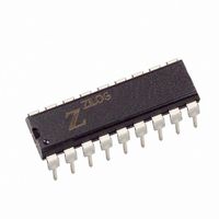
Z8622912PSC Zilog, Z8622912PSC Datasheet - Page 10

Z8622912PSC
Manufacturer Part Number
Z8622912PSC
Description
IC CCD W/2ND I2C ADD 18-DIP
Manufacturer
Zilog
Type
Video Decoderr
Datasheet
1.Z8622912PSC.pdf
(52 pages)
Specifications of Z8622912PSC
Applications
Set-Top Boxes, TV
Voltage - Supply, Digital
4.75 V ~ 5.25 V
Mounting Type
Through Hole
Package / Case
18-DIP (0.300", 7.62mm)
Processor Series
Z8622x
Core
Z80
Data Bus Width
8 bit
Program Memory Size
3.7 B
Maximum Clock Frequency
12 MHz
Number Of Programmable I/os
18
Operating Supply Voltage
4.75 V to 5.25 V
Maximum Operating Temperature
+ 70 C
Mounting Style
Through Hole
Minimum Operating Temperature
0 C
Lead Free Status / RoHS Status
Contains lead / RoHS non-compliant
Voltage - Supply, Analog
-
Lead Free Status / Rohs Status
No RoHS Version Available
Available stocks
Company
Part Number
Manufacturer
Quantity
Price
Part Number:
Z8622912PSC
Manufacturer:
ZILOG
Quantity:
20 000
< $ . 1 % - & + # ) 4 # / & ' 5 % 4 + 2 6 + 1 0
HSQR. These timing signals are used in the data output (dis-
play) circuits.
The H signal is further divided in the LINE and FLD CNTR
to produce the various decodes used to establish vertical
lock, time displays, and control functions required for prop-
er operation. The H signal is also used to generate the
Smooth Scroll timing signal for display.
The V Lock circuits produce a noise free vertical pulse de-
rived from the horizontal timing signal. When the user se-
lects Video as the vertical lock source, the internal synchro-
nizing signals are phased up with the incoming video by
comparing the internally generated vertical pulse to an input
vertical pulse. These pulses are derived from the Comp Sync
signal provided by the Sync Slicer. In the vertical lock set
to V
derived from Comp Sync. In either case, when proper phas-
ing has been established, this circuit outputs the LOCK sig-
nal which is used to provide additional noise immunity to
the slicing circuits.
The LOCKed state is established only after several succes-
sive fields have occurred and the two vertical pulses remain
in sync. When LOCKed, the internal timing will flywheel
until the timing of the two vertical pulses lose coincidence
for a number of consecutive fields. Until LOCK is estab-
lished, the decoder operates on a pulse-by-pulse basis.
Command Processor
The Command Processor circuit controls the manipulation
of the data for storage and display. This circuit processes
the Control Port input commands to determine the display
status required and the data channel selected. During the dis-
play time (lines 43–237), this information is used to control
the loading, addressing, clearing of the Display RAM, and
the operations of the Character ROM and Output Logic cir-
cuits.
During data recovery time (TV lines 21–42), the Command
Processor, in conjunction with the data recovery circuits, re-
covers the XDS data and the data for the selected data chan-
nel. Data is sent to the RAM for storage and display and/or
to the serial port, as appropriate. Where necessary, the Com-
mand Processor converts the input data to the appropriate
form.
IN
mode, the V
IN
signal is used in place of the signal
% Q P V K P W G F
Output Logic
The Output Logic circuits operate together to generate the
output color signals RED, GREEN and BLUE, and the Box
signal. When MONOchrome mode is selected, all three col-
or outputs carry the luminance information. These outputs
are positive output logic signals.
The character ROM contains the dot pattern for all the char-
acters. The output logic provides the hardware underline,
graphics characters, and the Italics slant-generator circuits.
The smooth scroll display is achieved by the smooth scroll
counter logic, which controls the addressing of the Charac-
ter ROM.
Decoder Control Circuit
The Decoder Control Circuit block is the users communi-
cations port. The circuit converts the information provided
to the control port into the necessary internal control signals
required to establish the operating mode of the decoder. This
port can be operated in one of two serial modes. The SMS
pin is used to establish either of the two serial control modes.
In the two wire (I
to its slave address for both the read and write conditions.
If the read bit is Low (indicating a WRITE sequence), then
the Z86229 responds with an acknowledge. The master
should then send an address byte followed by a data byte.
If the read bit is High (indicating a READ sequence), then
the Z86229 responds with an acknowledge followed by a
status byte and a data byte, respectively. Read data, how-
ever, is only available through indirect addressing; write ad-
dressing exhibits both indirect and direct modes. The busy
bit in the status byte indicates whether the write operation
has been completed or if read data is available.
The SPI mode is a three wire bus with the Z86229 acting
as the slave device. Communication is synchronized by the
SCK signal generated by the master. Typically, the serial
data output is transmitted on the falling edge of SCK and
the received data is captured on the rising edge of SCK. All
data is exchanged as 8-bit bytes.
Voltage/Current Reference
The Voltage/Current Reference circuit uses an externally-
connected resistor to establish the reference levels that are
used throughout the Z86229. For a minimal cost, an external
resistor can provide improved internal precision.
2
C) control mode, the Z86229 responds
ZiLOG


