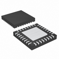
MAX9526ATJ+ Maxim Integrated Products, MAX9526ATJ+ Datasheet - Page 18

MAX9526ATJ+
Manufacturer Part Number
MAX9526ATJ+
Description
IC VID DECODER NTSC/PAL 32-TQFN
Manufacturer
Maxim Integrated Products
Type
Video Decoderr
Datasheet
1.MAX9526AEI.pdf
(38 pages)
Specifications of MAX9526ATJ+
Applications
Automotive Systems, Players, TV
Voltage - Supply, Analog
1.8V
Voltage - Supply, Digital
1.8V
Mounting Type
Surface Mount
Package / Case
32-TQFN Exposed Pad
Lead Free Status / RoHS Status
Lead free / RoHS Compliant
Low-Power, High-Performance
NTSC/PAL Video Decoder
Multiple asynchronous video input signals can be
decoded synchronously using multiple MAX9526s in
asynchronous (async) sampling mode. Figure 7 shows
an example of decoding four video input signals.
The MAX9526 is configured for async sampling mode
by writing the following registers:
When the MAX9526 is in async sampling mode, the
data outputs, D9–D0, of all decoders are synchronous
with the input clock (XTAL/OSC). The video content in
the data outputs is not frame aligned because the video
sources into each MAX9526 is asynchronous. A small
FPGA can be implemented to multiplex all four chan-
nels into a single 8- or 10-bit bus. This FPGA can also
format the outputs to be compatible for input into a
compression processor, which is commonly used in
digital video recorders (DVRs).
The crystal oscillator (external or internal) must have
better than ±50ppm accuracy for acceptable decoding
in this mode. An accuracy of ±10ppm is recommended
for optimal performance.
Recommended crystal parameters are shown in Table 3.
For systems where additional power-supply isolation is
required, the circuit shown in Figure 8 can be used.
Additional supply decoupling is added and analog
power (AVDD) isolation is increased with the use of a fer-
rite bead (FB). The analog ground connection (AGND)
should be connected to a separate ground plane that
has a small bridge to the main ground plane of the sys-
tem. The video input termination (V
ence (V
should also be connected to the AGND ground plane.
Table 3. Recommended Crystal Parameters
SMBus is a trademark of Intel Corp.
18
Frequency
Maximum Crystal ESR
Accuracy
Register 0x0D, B3 (XTAL_DIS) = 1 (disables the
crystal oscillator)
Register 0x0E, B5-4 (LLC_MODE) = 11 (forces
sampling to async mode)
______________________________________________________________________________________
REF
PARAMETER
Recommended Crystal Parameters
) decoupling, and AVDD supply decoupling
Applications Information
Multiple Decoder Operation
Power-Supply Decoupling
Fundamental mode only
Room temperature
Line-locked mode
Async mode with multiple decoders
IN1
/V
IN2
), video refer-
CONDITIONS
The MAX9526 features an I
2-wire serial interface consisting of a serial-data line
(SDA) and a serial-clock line (SCL). SDA and SCL facili-
tate communication between the MAX9526 and the
master at clock rates up to 400kHz. Figure 10 shows
the 2-wire interface timing diagram. The master gener-
ates SCL and initiates data transfer on the bus. The
master device writes data to the MAX9526 by transmit-
ting the proper slave address followed by the register
address and then the data word. Each transmit
sequence is framed by a START (S) or REPEATED
START (Sr) condition and a STOP (P) condition. Each
word transmitted to the MAX9526 is 8 bits long and is
followed by an acknowledge clock pulse. A master
reading data from the MAX9526 transmits the proper
slave address followed by a series of nine SCL pulses.
The MAX9526 transmits data on SDA in sync with the
master-generated SCL pulses. The master acknowl-
edges receipt of each byte of data. Each read
sequence is framed by a START or REPEATED START
condition, a not acknowledge, and a STOP condition.
SDA operates as both an input and an open-drain out-
put. A pullup resistor, typically greater than 500Ω, is
required on SDA. SCL operates only as an input. A
pullup resistor, typically greater than 500Ω, is required
on SCL if there are multiple masters on the bus, or if the
single master has an open-drain SCL output. Series
resistors in line with SDA and SCL are optional. Series
resistors protect the digital inputs of the MAX9526 from
high-voltage spikes on the bus lines, as well as mini-
mize crosstalk and undershoot of the bus signals.
One data bit is transferred during each SCL cycle. The
data on SDA must remain stable during the high period
of the SCL pulse. Changes in SDA while SCL is high
are control signals (see the START and STOP
Conditions section).
SDA and SCL idle high when the bus is not in use. A
master initiates communication by issuing a START con-
dition. A START condition is a high-to-low transition on
SDA with SCL high. A STOP condition is a low-to-high
MIN
START and STOP Conditions
2
C/SMBus™-compatible,
I
27.000
2
TYP
±50
±50
C Serial Interface
30
MAX
Bit Transfer
UNITS
MHz
ppm
Ω


