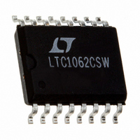
LTC1062CSW#PBF Linear Technology, LTC1062CSW#PBF Datasheet - Page 3

LTC1062CSW#PBF
Manufacturer Part Number
LTC1062CSW#PBF
Description
IC FILTR 5TH ORDR LOWPASS 16SOIC
Manufacturer
Linear Technology
Datasheet
1.LTC1062CN8PBF.pdf
(16 pages)
Specifications of LTC1062CSW#PBF
Filter Type
Butterworth, Lowpass Switched Capacitor
Frequency - Cutoff Or Center
20kHz
Number Of Filters
1
Max-order
5th
Voltage - Supply
5 V ~ 16 V, ±2.5 V ~ 8 V
Mounting Type
Surface Mount
Package / Case
16-SOIC (0.300", 7.5mm Width)
Ic Filter Type
Switched Capacitor
Filter Order
5th
No. Of Filters
1
Cutoff Frequency
20kHz
Program Clock Frequency Typ
4MHz
Supply Voltage Range
± 2.5V To ± 9V
Rohs Compliant
Yes
Lead Free Status / RoHS Status
Lead free / RoHS Compliant
Available stocks
Company
Part Number
Manufacturer
Quantity
Price
ELECTRICAL CHARACTERISTICS
ture range, otherwise specifications are at T
Figure 1.
PARAMETER
Internal Buffer
Bias Current
Offset Voltage
Voltage Swing
Short-Circuit Current Source/Sink
Clock (Note 3)
Internal Oscillator Frequency
Max Clock Frequency
Pin 5 (Pin 11 in SW16) Source or Sink Current
Note 1: Absolute Maximum Ratings are those values beyond which the life of
a device may be impaired.
Note 2: f
signal.
TYPICAL PERFOR A CE CHARACTERISTICS
–100
–20
–30
–40
–50
–60
–70
–80
–90
–10
0
0.1
Amplitude Response Normalized
to the Cutoff Frequency
V
T
2πRC
C
A
S
1
is the frequency where the gain is –3dB with respect to the input
= 25°C
= ±2.5V
f
=
f
CLK
CLK
1.62
f
f
C
= 250kHz, f
= 500kHz, f
CLK
f
CLK
= 100kHz, f
= 10kHz, f
f
CLK
f
IN
1
C
C
/f
= 2.5kHz
= 1kHz, f
C
= 5kHz
C
= 1kHz
C
= 100Hz
C
= 10Hz
W
1062 G01
U
10
CONDITIONS
R
C
A
LOAD
OSC
= 25°C. V
(Pin 5 to V
–100
–20
–30
–40
–50
–60
–70
–80
–90
= 20k
–10
0
0.1
Amplitude Response Normalized
to the Cutoff Frequency
V
T
2πRC
A
S
1
+
= 25°C
= ±2.5V
= 5V, V
–
f
=
, Pin 11 in SW16) = 100pF
f
CLK
The
CLK
1.62
f
f
C
= 250kHz, f
= 500kHz, f
CLK
f
CLK
–
= 100kHz, f
denotes specifications which apply over the full operating tempera-
= – 5V, unless otherwise specified, AC output measured at Pin 7,
= 10kHz, f
f
CLK
f
IN
1
Note 3: The external or driven clock frequency is divided by either 1, 2 or 4
depending upon the voltage at Pin 4. For the N8 package, when Pin 4 = V
ratio = 1; when Pin 4 = GND, ratio = 2; when Pin 4 = V
C
C
/f
= 2.5kHz
= 1kHz, f
C
= 5kHz
C
= 1kHz
C
= 100Hz
C
= 10Hz
1062 G01
10
–0.2
–0.4
–0.6
–0.8
–1.0
0.4
0.2
0
0.1
Passband Gain
vs Input Frequency
V
T
f
CLK
S
A
= ±5V
= 25°C
= 100kHz
±3.5
MIN
25
15
2πRC
0.2
1
=
±3.8
40/3
TYP
170
1.62
32
40
2
2
4
2πRC
f
C
f
IN
1
LTC1062
/f
–
C
=
, ratio = 4.
0.4
1000
MAX
1.6
2πRC
50
20
50
65
80
f
C
1
=
0.6
1.64
f
C
UNITS
0.8
1062 G03
1062fd
3
MHz
kHz
kHz
mV
mA
pA
pA
µA
+
V
1
,


