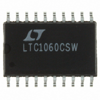
LTC1060CSW#PBF Linear Technology, LTC1060CSW#PBF Datasheet - Page 19

LTC1060CSW#PBF
Manufacturer Part Number
LTC1060CSW#PBF
Description
IC FILTER BUILDING BLOCK 20-SOIC
Manufacturer
Linear Technology
Datasheet
1.LTC1060CNPBF.pdf
(20 pages)
Specifications of LTC1060CSW#PBF
Filter Type
Universal Switched Capacitor
Frequency - Cutoff Or Center
30kHz
Number Of Filters
2
Max-order
4th
Voltage - Supply
±2.37 V ~ 5 V
Mounting Type
Surface Mount
Package / Case
20-SOIC (7.5mm Width)
Lead Free Status / RoHS Status
Lead free / RoHS Compliant
Available stocks
Company
Part Number
Manufacturer
Quantity
Price
PACKAGE DESCRIPTIO
Output Offsets
The DC offset at the filter bandpass output is always equal
to V
(Notch and LP) depend on the mode of operation and
external resistor ratios. Table 5 illustrates this.
It is important to know the value of the DC output offsets,
especially when the filter handles input signals with large
Table 5
LTC1060 OFFSETS
MODE
3, 4a
2, 5
1,4
(7.620 – 8.255)
(0.203 – 0.381)
OS3
1a
1b
1c
2a
2b
(
8.255
.300 – .325
.008 – .015
.325
. The DC offsets at the remaining two outputs
+.035
–.015
+0.889
–0.381
)
V
V
V
V
[V
• [R4/(R2 + R4)] + V
V
[V
•
[V
•
OS1
OS1
OS1
OS1
OS2
OS1
OS1
OS1
R2 + R4(1 + k)
R2 + R4k
NOTE:
1. DIMENSIONS ARE
*THESE DIMENSIONS DO NOT INCLUDE MOLD FLASH OR PROTRUSIONS.
[(1/Q) + 1 + ||H
[1 + (1/Q)] – V
[(1/Q) + 1 + R2/R1] – V
[(1/Q) + 1 + R2/R1] – V
R4(1 + k)
(1 + R2/R1 + R2/R3 + R2/R4) – V
R4k
(1 + R2/R1 + R2/R3 + R2/R4) – V
(1 + R2/R1 + R2/R3 + R2/R4) – V
MOLD FLASH OR PROTRUSIONS SHALL NOT EXCEED .010 INCH (0.254mm)
(6.477 ± 0.381)
.255 ± .015*
+ V
OS2
MILLIMETERS
+ V
PIN 3 (18)
OS3
OS2
OLP
INCHES
Information furnished by Linear Technology Corporation is believed to be accurate and reliable.
However, no responsibility is assumed for its use. Linear Technology Corporation makes no represen-
tation that the interconnection of its circuits as described herein will not infringe on existing patent rights.
R2 + R4k
V
OS2
20
/Q
1
OSN
[R2/(R2 + R4)]
||] – V
R2
R2 + R4(1 + k)
19
2
OS3
OS3
OS3
U
18
/Q
/Q
3
/Q
;k =
R2
17
4
R5 + R6
OS3
20-Lead PDIP (Narrow .300 Inch)
16
R6
(Reference LTC DWG # 05-08-1510)
OS3
OS3
(26.416)
5
1.040*
(R2/R3)]
MAX
;k =
(R2/R3)]
(R2/R3)]
15
6
R5 + R6
14
7
R6
N Package
13
8
12
9
dynamic range. As a rule of thumb, the output DC offsets
increase when:
11
10
PIN 2 (19)
1. The Q’s decrease.
2. The ratio (f
V
(0.508)
V
V
V
V
V
V
V
V
.020
done by decreasing either the (R2/R4) or the
R6/(R5 + R6) resistor ratios.
OSBP
MIN
OS3
OS3
OS3
OS3
OS3
OS3
OS3
OS3
(3.175 – 3.683)
.125 – .145
(3.048)
.120
MIN
CLK
V
V
~ (V
V
~ (V
~(V
~ (V
V
– V
OSN
OSN
OSN
OS1
/f
OS3
OSN
OSN
OSN
OSN
(0.127)
0
– V
– V
– V
.005
MIN
) increases beyond 100:1. This is
1 +
– V
– V
– V
– V
OS2
OS2
OS2
R4
R3
R4
R1
OS2
OS2
OS2
OS2
(2.54)
.100
BSC
) (1 + R5/R6)
) (1 + R5/R6)
(1.143 – 1.651)
PIN 1 (20)
+
)
)
.045 – .065
(R5 + 2R6)
(R5 + 2R6)
(R5 + R6)
(R5 + R6)
V
R4
R2
OSLP
+
R4
R3
– V
LTC1060
OS2
(0.457 ± 0.076)
R4
R2
.018 ± .003
19
1060fb
(1.651)
.065
TYP
N20 1002


