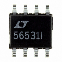
LTC1565-31IS8#PBF Linear Technology, LTC1565-31IS8#PBF Datasheet - Page 7

LTC1565-31IS8#PBF
Manufacturer Part Number
LTC1565-31IS8#PBF
Description
IC FILTR 7TH ORDER 650KHZ 8-SOIC
Manufacturer
Linear Technology
Datasheet
1.LTC1565-31CS8PBF.pdf
(12 pages)
Specifications of LTC1565-31IS8#PBF
Filter Type
Linear Phase, Continuous-Time Lowpass
Frequency - Cutoff Or Center
650kHz
Number Of Filters
1
Max-order
7th
Voltage - Supply
4.75 V ~ 11 V, ±4.75 V ~ 5.5 V
Mounting Type
Surface Mount
Package / Case
8-SOIC (3.9mm Width)
Lead Free Status / RoHS Status
Lead free / RoHS Compliant
Available stocks
Company
Part Number
Manufacturer
Quantity
Price
APPLICATIONS INFORMATION
input voltages are Pin 1 = 2.5V DC ±0.5V and Pin 2 = 2.5V
DC ±0.5V. Also note Figure 5 shows a 78dB SNR ratio for
higher THD levels.
As seen in Figures 3 and 4, the spurious free dynamic
range can be optimized by setting the input common mode
voltage slightly below one-half of the power supply voltage,
i.e., 2V for a single 5V supply and –0.5V for a ±5V supply.
Figure 6 shows the THD and SNR ratio versus differential
input voltage level for both a single 5V supply and a ±5V
supply when the common mode input voltage is 2V and
–0.5V respectively.
For best performance, the inputs should be driven dif-
ferentially. For single-ended signals, connect the unused
input to Pin 3 or a common mode reference.
–30
–40
–80
–90
–30
–40
–80
–90
–50
–60
–70
–50
–60
–70
Figure 5. Dynamic Range Diff-In, Diff-Out
Figure 6. THD vs V
Input Voltage 0.5V Below Mid Supply
0.5
0.5
f
f
IN
IN
DIFFERENTIAL INPUT VOLTAGE (V
= 100kHz
= 100kHz
1.0
1.0
THD: V
THD: V
SNR
THD: V
THD: V
SNR
DIFFERENTIAL INPUT (
S
S
1.5
1.5
S
S
= 5V, V
= ±5V, V
= 5V, V
= ±5V, V
IN
2.0
2.0
CM
CM
CM
CM
for a Common Mode
= 2.5V
= 2V
= 0V
= –0.5V
2.5
2.5
P-P
)
3.0
3.0
P-P
1565-31 F05
1565-31 F06
)
3.5
3.5
Output Common Mode and Differential Voltage Range
The output is a fully differential signal with a common mode
level equal to the voltage at Pin 3. The specifi cations in
the Electrical Characteristics table assume the inputs are
driven differentially and the output is observed differentially.
However, Pin 8 can be used as a single-ended output by
simply fl oating Pin 7. Pin 7 can be used as an inverting
single-ended output by fl oating Pin 8. Using Pins 7 or 8
as single-ended outputs will decrease the performance.
The common mode output voltage can be adjusted by over-
driving the voltage present on Pin 3. The best performance
is achieved using a common mode output voltage that is
equal to mid supply (the default Pin 3 voltage). Figures
7 and 8 illustrate the THD versus output common mode
voltage for a 2V
mode input voltage that is 0.5V below mid supply.
Figure 7. THD vs Common Mode Output Voltage
Figure 8. THD vs Common Mode Output Voltage
–40
–10
–20
–30
–50
–60
–70
–80
–10
–20
–30
–40
–50
–60
–80
–90
–70
0
0
1.0
–4
V
V
V
IN
S
IN(CM)
P-P
COMMON MODE OUTPUT VOLTAGE (V)
COMMON MODE OUTPUT VOLTAGE (V)
= ±5V
–3
= 2V
1.5
differential input voltage and a common
= –0.5V
P-P
–2
100kHz
2.0
–1
2.5
0
V
V
V
IN
S
IN(CM)
1
= 5V
3.0
= 2V
LTC1565-31
= 2V
P-P
2
3.5
100kHz
1565-31 F07
1565-31 F08
3
4.0
4
156531fa
7


