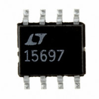
LTC1569CS8-7#PBF Linear Technology, LTC1569CS8-7#PBF Datasheet - Page 3

LTC1569CS8-7#PBF
Manufacturer Part Number
LTC1569CS8-7#PBF
Description
IC FILTER 10TH ORDR LOWPASS8SOIC
Manufacturer
Linear Technology
Datasheet
1.LTC1569CS8-7PBF.pdf
(12 pages)
Specifications of LTC1569CS8-7#PBF
Filter Type
Linear Phase, Lowpass Switched Capacitor
Frequency - Cutoff Or Center
300kHz
Number Of Filters
1
Max-order
10th
Mounting Type
Surface Mount
Package / Case
8-SOIC (3.9mm Width)
Lead Free Status / RoHS Status
Lead free / RoHS Compliant
Voltage - Supply
-
Available stocks
Company
Part Number
Manufacturer
Quantity
Price
The
V
Output DC Offset
(Note 2)
Output DC Offset Drift
Clock Pin Logic Thresholds
when Clocked Externally
Power Supply Current
(Note 3)
Power Supply Voltage where
Low Power Mode is Enabled
Clock Feedthrough
Wideband Noise
THD
Clock-to-Cutoff
Frequency Ratio
Max Clock Frequency
(Note 4)
Min Clock Frequency
(Note 5)
Input Frequency Range
Note 1: Absolute maximum ratings are those values beyond which the life
of a device may be impaired.
Note 2: DC offset is measured with respect to Pin 3.
Note 3: There are several operating modes which reduce the supply
current. For V
reduced by 50% relative to V
clock source and the divide-by-4 or divide-by-16 mode is enabled, the
supply current is typically reduced by 60%,relative to divide-by-1 mode,
independent of the value of V
ELECTRICAL C
PARAMETER
S
= 3V (V
denotes the specifications which apply over the full operating temperature range, otherwise specifications are at T
+
S
= 3V, V
< 4V, relative to divide-by-1 mode, the current is typically
–
= 0V), f
S
S
HARA TERISTICS
.
= 5V. If the internal oscillator is used as the
CONDITIONS
R
R
V
V
V
f
Pin 5 Open, 4), f
f
Pin 5 Shorted to Pin 4, 1), f
f
Pin 5 Shorted to Pin 4, 1), f
Pin 5 Shorted to Pin 4, Note 3
R
Noise BW = DC to 2 • f
f
V
V
V
3V to 5V, T
Aliased Components <–65dB
CLK
CLK
CLK
IN
CLK
EXT
EXT
S
S
S
EXT
S
S
S
= 3V
= 5V
= 5V
= 10kHz, 1.5V
= 3V
= 5V
= 5V
= 1.028MHz (10k from Pin 6 to Pin 7,
= 4.096MHz (10k from Pin 6 to Pin 7,
= 8.192MHz (5k from Pin 6 to Pin 7,
= 4.096MHz, f
= 10k, Pin 5 Shorted to Pin 4
= 10k, Pin 5 Shorted to Pin 4
= 10k, Pin 5 Open
C
A
< 85 C
P-P
CUTOFF
CUTOFF
CUTOFF
= 32kHz
= 128kHz, R
CUTOFF
CUTOFF
= 128kHz
= 256kHz
LOAD
Note 4: The maximum clock frequency is arbitrarily defined as the
frequency at which the filter AC response exhibits >1dB of gain peaking.
Note 5: The minimum clock frequency is arbitrarily defined as the frequecy
at which the filter DC offset changes by more than 5mV.
Note 6: Thermal resistance varies depending upon the amount of PC board
metal attached to the device.
covered with 2oz copper on both sides.
= 10k unless otherwise specified.
V
V
V
V
V
V
Min Logical “1”
Max Logical “0”
Min Logical “1”
Max Logical “0”
Min Logical “1”
Max Logical “0”
V
V
V
V
V
V
S
S
S
S
S
S
S
S
S
S
S
S
= 3V
= 5V
= 5V
= 3V
= 5V
= 5V
= 3V
= 5V
= 10V
= 3V
= 5V
= 10V
JA
is specified for a 2500mm
MIN
3.7
0.9 • f
– 25
– 25
TYP
125
2.6
0.5
4.0
0.5
4.0
0.5
9.5
4.2
0.4
9.6
20
27
74
32
13
6
7
9
5
3
LTC1569-7
15
25
2
6
CLK
MAX
4.6
A
10
13
14
14
30
37
2
8
9
9
12
5
test board
= 25 C.
mV
UNITS
V
3
V/ C
V/ C
V/ C
MHz
MHz
MHz
RMS
RMS
kHz
mV
mV
mV
mA
mA
mA
mA
mA
mA
mA
mA
mA
mA
mA
mA
dB
Hz
V
V
V
V
V
V
V


