LTC6605CDJC-7#PBF Linear Technology, LTC6605CDJC-7#PBF Datasheet
LTC6605CDJC-7#PBF
Specifications of LTC6605CDJC-7#PBF
Available stocks


Related parts for LTC6605CDJC-7#PBF


LTC6605CDJC-7#PBF Summary of contents
Page 1
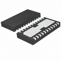
... The LTC6605-7 is available in a compact 6mm × 3mm 22-pin leadless DFN package and operates over a –40°C to 85°C temperature range. , LT, LTC and LTM are registered trademarks of Linear Technology Corporation. All other trademarks are the property of their respective owners. 120 3V – ...
Page 2
... Junction Temperature ........................................... 150°C Storage Temperature Range ................... –65°C to 150°C ORDER INFORMATION LEAD FREE FINISH TAPE AND REEL LTC6605CDJC-7#PBF LTC6605CDJC-7#TRPBF LTC6605IDJC-7#PBF LTC6605IDJC-7#TRPBF Consult LTC Marketing for parts specifi ed with wider operating temperature ranges. *The temperature grade is identifi label on the shipping container. ...
Page 3
DC ELECTRICAL CHARACTERISTICS temperature range, otherwise specifi cations are 10k. The fi lter is confi gured for a gain of 1, unless otherwise noted. V BAL V )/ defi ned ...
Page 4
LTC6605-7 AC ELECTRICAL CHARACTERISTICS temperature range, otherwise specifi cations are at T otherwise noted. Filter confi gured as in Figure 2, unless otherwise noted )/ defi ned –OUT INCM +IN –IN SYMBOL ...
Page 5
ELECTRICAL CHARACTERISTICS Note 8: See the Applications Information section for a detailed discussion of input and output common mode range. Input common mode range is tested by measuring the differential DC gain with V = mid-supply, and again with V ...
Page 6
LTC6605-7 TYPICAL PERFORMANCE CHARACTERISTICS Harmonic Distortion vs Frequency, BIAS High –40 DIFFERENTIAL INPUT, HD2 DIFFERENTIAL INPUT, HD3 –50 SINGLE-ENDED INPUT, HD2 SINGLE-ENDED INPUT, HD3 –60 –70 –80 –90 –100 –110 –120 0 100 FREQUENCY (MHz) 66057 G05 V ...
Page 7
TEST CIRCUITS LTC6605-7 400Ω 1 100Ω INP – BIAS 3 – V INM 100Ω 400Ω 5 LTC6605-7 1μF 400Ω V +IN 1 100Ω BIAS 3 IN – 100Ω 4 1μF 400Ω V ...
Page 8
LTC6605-7 PIN FUNCTIONS +IN4 A, –IN4 A, +IN4 B, –IN4 B (Pins 11): Inputs to Trimmed 400Ω Resistors. Can accept an input signal, be fl oated, tied to an output pin, or connected to external components. +IN1 ...
Page 9
BLOCK DIAGRAM +IN4 A 1 +IN1 A 2 BIAS A 3 –IN1 A 4 –IN4 A 5 – +IN4 B 7 +IN1 B 8 BIAS B 9 –IN1 –IN4 B 114.8pF 400Ω 400Ω 69.3pF 100Ω ...
Page 10
LTC6605-7 APPLICATIONS INFORMATION Functional Description The LTC6605-7 is designed to make the implementation of high frequency fully differential fi ltering functions very easy. Two very low noise amplifi ers are surrounded by precision matched resistors and precision matched capaci- tors ...
Page 11
APPLICATIONS INFORMATION Setting the passband gain (GAIN = R2/R1) only requires choosing a value for R1, since fi xed internal 400Ω. Therefore, the following three gains can be easily confi gured without external components: Table 1. Confi ...
Page 12
LTC6605-7 APPLICATIONS INFORMATION – – 66057 F04a f = 6.5MHz –3dB GAIN = 1V/ V (0dB 800Ω IN Gain Response –10 ...
Page 13
APPLICATIONS INFORMATION 80.6Ω 4 – 80.6Ω 10 – 66057 F05a ±0.4dB 6.7MHz PASSBAND GAIN = 1V/ V (0dB 800Ω IN Gain Response –10 ...
Page 14
LTC6605-7 APPLICATIONS INFORMATION Input Impedance Calculating the low frequency input impedance depends on how the inputs are driven. Figure 6 shows a simplifi ed low frequency equivalent cir- cuit. For balanced input sources (V frequency input impedance is given by ...
Page 15
APPLICATIONS INFORMATION Noise When comparing the LTC6605-7’s noise to that of other amplifi ers, be sure to compare similar specifi cations. Stand- alone op amps often specify noise referred to the inputs of the op amp. The LTC6605-7’s internal op ...
Page 16
LTC6605-7 APPLICATIONS INFORMATION For split power supplies recommended that addi- tional high quality X5R or X7R, 0.1μF capacitors be used + – to bypass pin V to ground and V minimal routing. For driving heavy differential loads (< ...
Page 17
APPLICATIONS INFORMATION the sampling transient of the ADC (see Figure 8). The capacitance serves to provide the bulk of the charge during the sampling process, while the two resistors at the outputs of the LTC6605-7 are used to dampen and ...
Page 18
LTC6605-7 TYPICAL APPLICATIONS V INA V INB THREE GAINS ARE POSSIBLE, AS SHOWN IN FIGURE 4 18 Dual, Matched, 4th Order 7MHz Lowpass Filter LTC6605-7 LTC6605 243Ω – – ...
Page 19
... MOLD FLASH. MOLD FLASH, IF PRESENT, SHALL NOT EXCEED 0.15mm ON ANY SIDE Information furnished by Linear Technology Corporation is believed to be accurate and reliable. However, no responsibility is assumed for its use. Linear Technology Corporation makes no representa- tion that the interconnection of its circuits as described herein will not infringe on existing patent rights. ...
Page 20
... Lowpass and Bandpass Responses Up to 10MHz 1.5nV/√Hz Noise, –95dBc Distortion at 10MHz 1.6nV/√Hz Noise, –72dBc Distortion at 50MHz, 18mA Cut-Off Frequencies of 2.5MHz/5MHz/10MHz/15MHz/20MHz 7MHz to 25MHz Pin-Confi gurable Cut-Off Frequencies of 2.5MHz or 5MHz www.linear.com ● V OUTA V OUTB 100 LT 1208 • PRINTED IN USA © LINEAR TECHNOLOGY CORPORATION 2008 66057f ...