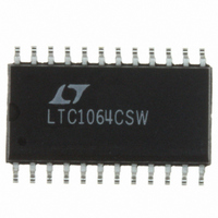
LTC1064CSW#PBF Linear Technology, LTC1064CSW#PBF Datasheet - Page 8

LTC1064CSW#PBF
Manufacturer Part Number
LTC1064CSW#PBF
Description
IC FILTR BUILDNG BLK QUAD 24SOIC
Manufacturer
Linear Technology
Datasheet
1.LTC1064CNPBF.pdf
(20 pages)
Specifications of LTC1064CSW#PBF
Filter Type
Universal Switched Capacitor
Frequency - Cutoff Or Center
140kHz
Number Of Filters
4
Max-order
8th
Voltage - Supply
±2.375 V ~ 8 V
Mounting Type
Surface Mount
Package / Case
24-SOIC (7.5mm Width)
Lead Free Status / RoHS Status
Lead free / RoHS Compliant
Available stocks
Company
Part Number
Manufacturer
Quantity
Price
LTC1064
APPLICATIONS
8
Offset Nulling
Lowpass filters may have too much DC offset for some
users. A servo circuit may be used to actively null the
offsets of the LTC1064 or any LTC switched-capacitor
filter. The circuit shown in Figure 4 will null offsets to better
than 300µV. This circuit takes seconds to settle because of
the integrator pole frequency.
W
PRIMARY MODES
Mode 1
In Mode 1, the ratio of the external clock frequency to the
center frequency of each 2nd order section is internally
fixed at 50:1 or 100:1. Figure 5 illustrates Mode 1 provid-
ing 2nd order notch, lowpass and bandpass outputs.
Mode 1 can be used to make high order Butterworth
lowpass filters; it can also be used to make low Q notches
and for cascading 2nd order bandpass functions tuned at
the same center frequency with unity gain. Mode 1 is faster
than Mode 3. Note that Mode 1 can only be implemented
with three of the four LTC1064 sections because Section
D has no externally available summing node. Section D,
however, can be internally connected in Mode 1 upon
special request.
V
V
POSITIVE
SUPPLY
+
IN
TRACE FOR FILTER
ODES OF OPERATIO
Figure 3. Buffering the Output of a 4th Order Bandpass Realization
R11
SEPARATE V
0.1µF
R31
R21
U
7
+
POWER SUPPLY TRACE FOR BUFFER
INFORMATION
U
LTC1064
W
19
U
0.1µF
R22
R32
R12
10k
NEGATIVE
SUPPLY
U
0.1µF
–
+
LT
LT1007
LT1056
®
318
4
7
0.1µF
V
Noise
All the noise performance mentioned excludes the clock
feedthrough. Noise measurements will degrade if the
already described grounding bypassing and buffering
techniques are not practiced. The graph Wideband Noise
vs Q in the Typical Performance Characteristics section is
a very good representation of the noise performance of
this device.
10k
IN
+
1µF
R1
Figure 5. Mode 1: 2nd Order Filter Providing Notch,
Bandpass and Lowpass
+
1064 F03
V
OUT
f
O
=
1µF
100(50)
AGND
f
C1 = C2 = LOW LEAKAGE FILM
R1 = R2 = METAL FILM 1%
CLK
FIRST SUMMING
–
+
; f
TO FILTER
n
R3
R2
= f
(I.E., POLYPROPYLENE)
NODE
O
; H
OLP
Figure 4. Servo Amplifier
= –
100k
R3
R2
R1
N
1/4 LTC1064
+
; H
OBP
Σ
–
S
= –
0.1µF
R3
R1
LT1012
∫
C2
; H
ON1
+
–
= –
FILTER OUTPUT
BP
R2
R1
∫
R2
1M
FROM
; Q =
R1
1M
1064 F05
C1
0.1µF
1064fb
R3
R2
1064 F04
LP


